

This article will discuss five VHDL programming problems in the VIVADO environment.
Before diving into this VHDL tutorial, we assume that you have a basic understanding of electronics fundamentals, such as counters, encoders, decoders, and 7-segment displays.
Topic list (click to jump)
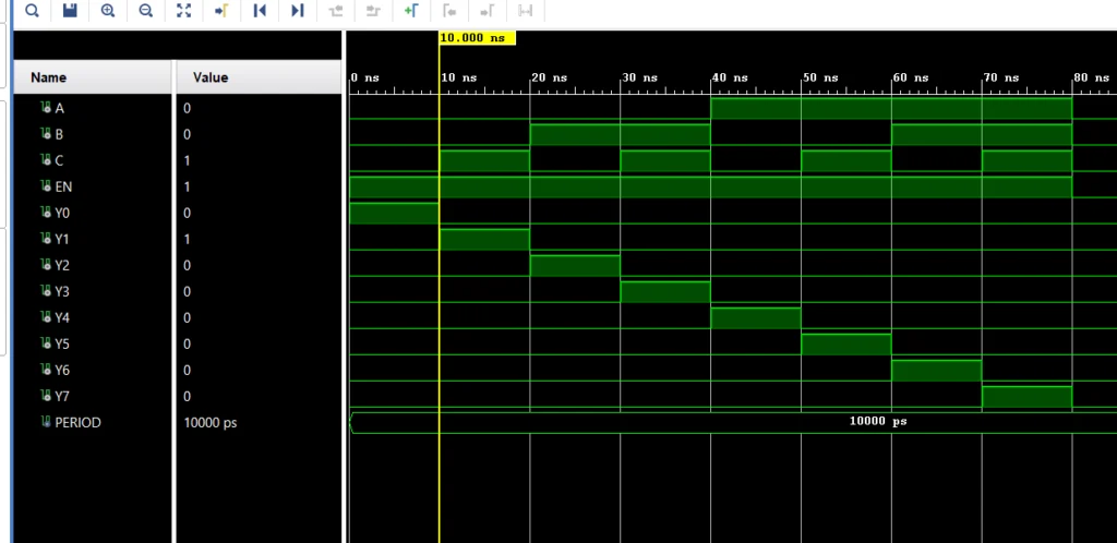
- (VHDL tutorial 1.0)-Create a concurrent instruction 3 to 8 decoder (enable: active high). Make a test bench, then simulate your design on it.
- (VHDL tutorial 2.0)-Design the 74AS245 bidirectional buffer using the table and logic circuit
- (VHDL tutorial 3.0)-Design a hexadecimal to 7−segment decoder
- (VHDL turotial 4.0)-Design a Hexadecimal counter (0−F) with inputs
- (VHDL turotial 5.0)-Design an Up/Down BCD counter (0−9) with inputs
Under these VHDL tutorial topics, we include some basic electronic explanations.
1. (VHDL tutorial 1.0) – Create a concurrent instruction 3 to 8 decoder (enable: active high). Make a test bench, then simulate the design on it.
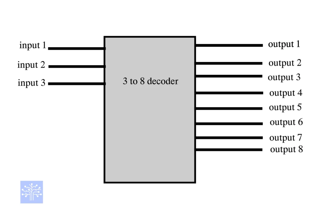
3 to 8 decoder
We have 3 inputs to create 8 different combinations using a decoder. In reality, we use this type of decoder to reduce the number of inputs. When the ‘enable’ signal is active high, it means it becomes active only when we provide a high input value, which is ‘1’
This is the basis diagram for 3 to 8 decoder
Truth table
| A0 | A1 | A3 | D0 | D1 | D2 | D3 | D4 | D5 | D6 | D7 |
| 0 | 0 | 0 | 1 | 0 | 0 | 0 | 0 | 0 | 0 | 0 |
| 0 | 0 | 1 | 0 | 1 | 0 | 0 | 0 | 0 | 0 | 0 |
| 0 | 1 | 0 | 0 | 0 | 1 | 0 | 0 | 0 | 0 | 0 |
| 0 | 1 | 1 | 0 | 0 | 0 | 1 | 0 | 0 | 0 | 0 |
| 1 | 0 | 0 | 0 | 0 | 0 | 0 | 1 | 0 | 0 | 0 |
| 1 | 0 | 1 | 0 | 0 | 0 | 0 | 0 | 1 | 0 | 0 |
| 1 | 1 | 0 | 0 | 0 | 0 | 0 | 0 | 0 | 1 | 0 |
| 1 | 1 | 1 | 0 | 0 | 0 | 0 | 0 | 0 | 0 | 1 |
Also, all the execution occurs during the enable bit being set to one.
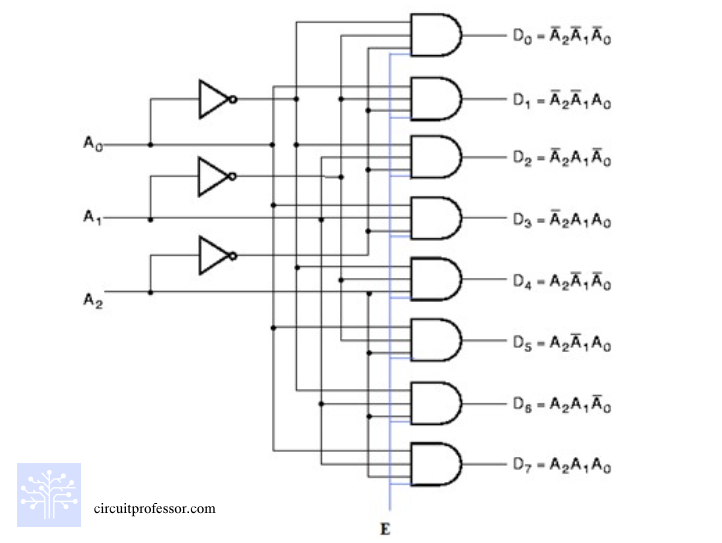
We can create a 3-to-8 decoder using two methods. The first method involves using two 2-to-4 decoders, while the alternative approach is to construct the decoder using basic logic building blocks such as AND and NOT gates.
In this VHDL tutorial, our focus lies on the decoder, utilizing fundamental logic building blocks like AND and NOT gates.
Block diagram
VHDL code for 3 to 8 decoder
library IEEE;
use IEEE.STD_LOGIC_1164.ALL;

entity Decoder_3to8 is
    Port (
        A, B, C : in  STD_LOGIC;
        EN : in STD_LOGIC;
        Y0, Y1, Y2, Y3, Y4, Y5, Y6, Y7 : out STD_LOGIC
    );
end Decoder_3to8;

architecture Behavioral of Decoder_3to8 is
begin
    process(A, B, C, EN)
    begin
        if EN = '1' then
            Y0 <= NOT (A) AND NOT (B) AND NOT (C);
            Y1 <= NOT (A) AND NOT (B) AND C;
            Y2 <= NOT (A) AND B AND NOT (C);
            Y3 <= NOT (A) AND B AND C;
            Y4 <= A AND NOT (B) AND NOT (C);
            Y5 <= A AND NOT (B) AND C;
            Y6 <= A AND B AND NOT (C);
            Y7 <= A AND B AND C;
        else
            Y0 <= '0';
            Y1 <= '0';
            Y2 <= '0';
            Y3 <= '0';
            Y4 <= '0';
            Y5 <= '0';
            Y6 <= '0';
            Y7 <= '0';
        end if;
    end process;
end Behavioral;
This is the easiest way of coding a 3-to-8 decoder.
Test bench
library IEEE;
use IEEE.STD_LOGIC_1164.ALL;

entity Testbench_Decoder_3to8 is
end Testbench_Decoder_3to8;

architecture Behavioral of Testbench_Decoder_3to8 is
    -- Constants
    constant PERIOD : time := 10 ns;

    -- Signals
    signal A, B, C, EN : std_logic := '0';
    signal Y0, Y1, Y2, Y3, Y4, Y5, Y6, Y7 : std_logic;

    -- Component instantiation
    component Decoder_3to8
        Port (
            A, B, C : in  STD_LOGIC;
            EN : in STD_LOGIC;
            Y0, Y1, Y2, Y3, Y4, Y5, Y6, Y7 : out STD_LOGIC
        );
    end component;

begin
    -- DUT (Device Under Test) instantiation
    DUT: Decoder_3to8
        port map (
            A => A,
            B => B,
            C => C,
            EN => EN,
            Y0 => Y0,
            Y1 => Y1,
            Y2 => Y2,
            Y3 => Y3,
            Y4 => Y4,
            Y5 => Y5,
            Y6 => Y6,
            Y7 => Y7
        );

    -- Stimulus process
    stim_proc: process
    begin
        A <= '0'; B <= '0'; C <= '0'; EN <= '1';
        wait for PERIOD;

        A <= '0'; B <= '0'; C <= '1'; EN <= '1';
        wait for PERIOD;

        A <= '0'; B <= '1'; C <= '0'; EN <= '1';
        wait for PERIOD;

        A <= '0'; B <= '1'; C <= '1'; EN <= '1';
        wait for PERIOD;

        A <= '1'; B <= '0'; C <= '0'; EN <= '1';
        wait for PERIOD;

        A <= '1'; B <= '0'; C <= '1'; EN <= '1';
        wait for PERIOD;

        A <= '1'; B <= '1'; C <= '0'; EN <= '1';
        wait for PERIOD;

        A <= '1'; B <= '1'; C <= '1'; EN <= '1';
        wait for PERIOD;

        -- Disable the decoder
        A <= '0'; B <= '0'; C <= '0'; EN <= '0';
        wait;
    end process;
end Behavioral;
After RTL analysis, this type of circuit diagram will be generated
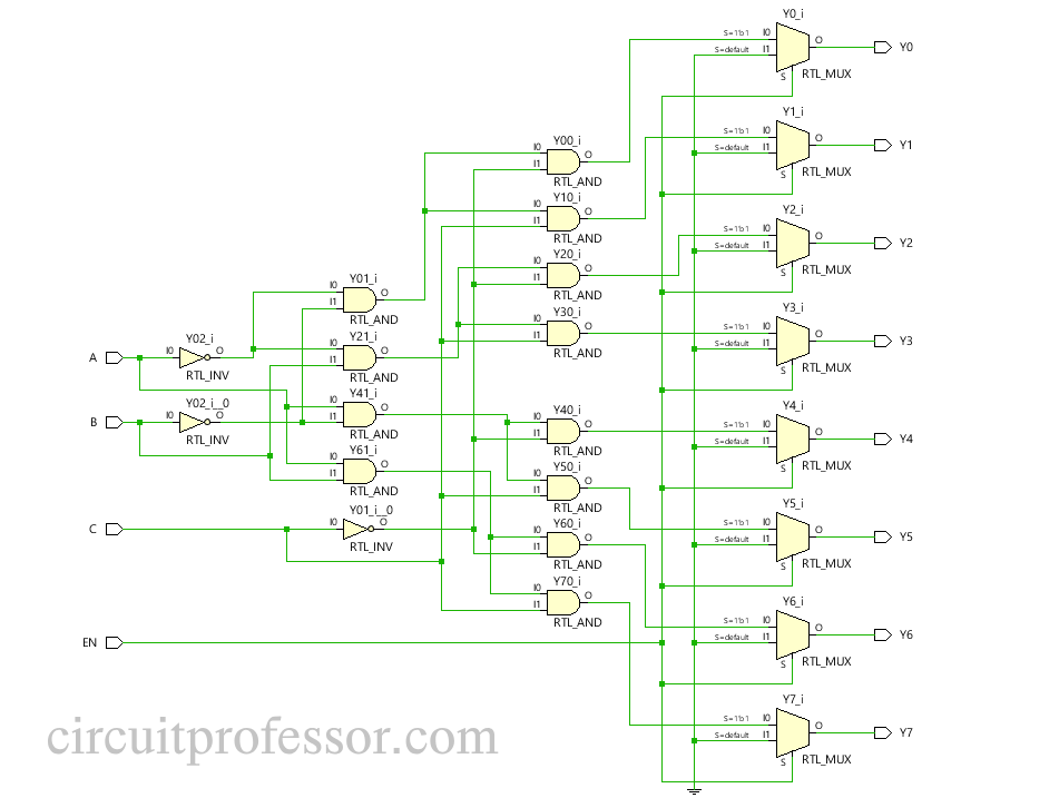
In reality, we don’t have a 4-input AND gate available inside an FPGA board. Therefore, when we create the code, the RTL (Register-Transfer Level) synthesizer automatically uses MUXes and additional 2-input AND gates to implement the functionality. As a result, the final design may not resemble the previous block diagram exactly, but the synthesized version will still accomplish the intended logic.
Simulation window
This is the first part of the VHDL tutorial.
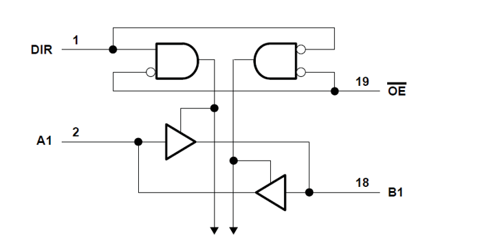
2.(VHDL tutorial 2.0)-Design the 74AS245 bidirectional buffer using the table and logic circuit
74AS245
A specific integrated circuit (IC) chip from the 74AS family is identified by the designation “74AS245”. A popular octal (8-bit) bidirectional bus transceiver is the 74AS245
74AS245 diagram
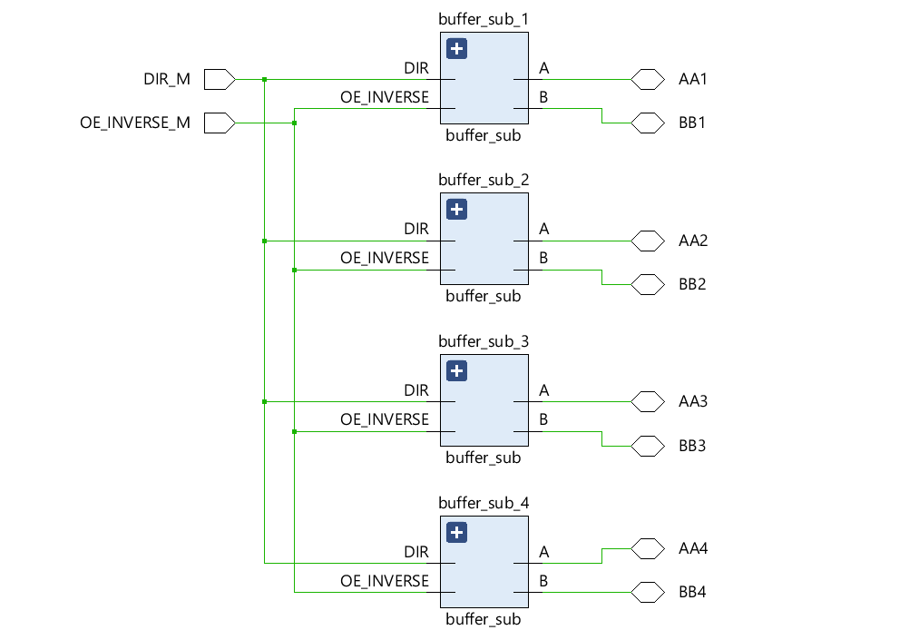
Additionally, we extend this circuit to an 8-bit configuration. Therefore, we need to create a common element separately in a separate VHDL file and then import it into our main code.
Note: In this code, we have extended the design to work with 4-bit data.
Truth table
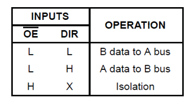
By setting the values of DIR to low and OE to high, we can alter the data direction through the circuit.
VHDL code for common module
library IEEE;
use IEEE.STD_LOGIC_1164.ALL;


entity buffer_sub is
    Port (
        A, B : inout STD_LOGIC;
        OE_INVERSE, DIR : in STD_LOGIC
    );
end buffer_sub;

architecture Behavioral of buffer_sub is

begin
    process (OE_INVERSE, DIR)
    begin
        if OE_INVERSE = '0' then
            if DIR = '0' then
                -- B data goes to A data line
                A <= B;
            else
                --A data goes to B data line
                B <= A;
            end if;
        elsif OE_INVERSE = '1' then
            --douing nothing
        end if;

     end process;
end Behavioral;
VHDL code for final design
library IEEE;
use IEEE.STD_LOGIC_1164.ALL;


entity final_design is
    Port(
            AA1,BB1,AA2,BB2,AA3,BB3,AA4,BB4 : inout STD_LOGIC;
            OE_INVERSE_M, DIR_M : in STD_LOGIC
       );
end final_design;

architecture structural of final_design is
    -- Declare the signals to GO to another buffer
  signal intermediate_OE_INVERSE_M, intermediate_DIR_M : std_logic;
  component buffer_sub
    port (
      A, B : inout STD_LOGIC;
      OE_INVERSE, DIR : in STD_LOGIC
    );
  end component;


begin
-- Instantiate buffer
buffer_sub_1 : buffer_sub
    port map (
      A => AA1,
      B => BB1,
      OE_INVERSE => OE_INVERSE_M,
      DIR =>  DIR_M
    );

buffer_sub_2 : buffer_sub
    port map (
      A => AA2,
      B => BB2,
      OE_INVERSE => OE_INVERSE_M,
      DIR =>  DIR_M
    );
buffer_sub_3 : buffer_sub
    port map (
      A => AA3,
      B => BB3,
      OE_INVERSE => OE_INVERSE_M,
      DIR =>  DIR_M
    );

buffer_sub_4 : buffer_sub
    port map (
      A => AA4,
      B => BB4,
      OE_INVERSE => OE_INVERSE_M,
      DIR =>  DIR_M
    );


end structural;
After RTL analysis, this type of circuit diagram will be generated
Test bench
library IEEE;
use IEEE.STD_LOGIC_1164.ALL;

entity testbench_final_design is
end testbench_final_design;

architecture Behavioral of testbench_final_design is
    -- Constants
    constant PERIOD : time := 10 ns;

    -- Signals for the final_design entity
    signal AA1, BB1, AA2, BB2, AA3, BB3, AA4, BB4 : std_logic;
    signal OE_INVERSE_M, DIR_M : std_logic;

    -- Component instantiation for final_design
    component final_design
        Port(
            AA1, BB1, AA2, BB2, AA3, BB3, AA4, BB4 : inout STD_LOGIC;
            OE_INVERSE_M, DIR_M : in STD_LOGIC
       );
    end component;

    -- Component instantiation for buffer_sub
    component buffer_sub
        port (
            A, B : inout STD_LOGIC;
            OE_INVERSE, DIR : in STD_LOGIC
        );
    end component;

begin
    -- DUT (Device Under Test) instantiation
    DUT: final_design
        port map (
            AA1 => AA1,
            BB1 => BB1,
            AA2 => AA2,
            BB2 => BB2,
            AA3 => AA3,
            BB3 => BB3,
            AA4 => AA4,
            BB4 => BB4,
            OE_INVERSE_M => OE_INVERSE_M,
            DIR_M => DIR_M
        );

    -- Stimulus process
    stim_proc: process
    begin
        -- Initialize signals (you can modify these values as needed)
        AA1 <= '0'; BB1 <= '1';  -- Example values for AA1 and BB1
        AA2 <= '1'; BB2 <= '0';  -- Example values for AA2 and BB2
        AA3 <= '1'; BB3 <= '1';  -- Example values for AA3 and BB3
        AA4 <= '0'; BB4 <= '0';  -- Example values for AA4 and BB4
        OE_INVERSE_M <= '0';     -- Example value for OE_INVERSE_M (LOW)
        DIR_M <= '1';            -- Example value for DIR_M (HIGH)

        -- Wait for a few clock cycles to observe the behavior
        wait for 2 * PERIOD;

        -- Change the values of signals for B data to go to A
        AA1 <= '0'; BB1 <= '1';  -- Example values for AA1 and BB1 (no change)
        AA2 <= '1'; BB2 <= '0';  -- Example values for AA2 and BB2 (no change)
        AA3 <= '1'; BB3 <= '1';  -- Example values for AA3 and BB3 (no change)
        AA4 <= '0'; BB4 <= '0';  -- Example values for AA4 and BB4 (no change)
        OE_INVERSE_M <= '0';     -- Example value for OE_INVERSE_M (LOW)
        DIR_M <= '0';            -- Example value for DIR_M (LOW)

        -- Wait for a few clock cycles to observe the behavior
        wait for 2 * PERIOD;

        -- Change the values of signals for A data to go to B
        AA1 <= '1'; BB1 <= '0';  -- Example values for AA1 and BB1 (switch data)
        AA2 <= '0'; BB2 <= '1';  -- Example values for AA2 and BB2 (switch data)
        AA3 <= '1'; BB3 <= '0';  -- Example values for AA3 and BB3 (switch data)
        AA4 <= '0'; BB4 <= '1';  -- Example values for AA4 and BB4 (switch data)
        OE_INVERSE_M <= '0';     -- Example value for OE_INVERSE_M (LOW)
        DIR_M <= '1';            -- Example value for DIR_M (HIGH)

        -- Wait for a few clock cycles to observe the behavior
        wait for 2 * PERIOD;

        -- Set OE_INVERSE to high for isolation case
        AA1 <= '0'; BB1 <= '1';  -- Example values for AA1 and BB1 (no change)
        AA2 <= '1'; BB2 <= '0';  -- Example values for AA2 and BB2 (no change)
        AA3 <= '1'; BB3 <= '1';  -- Example values for AA3 and BB3 (no change)
        AA4 <= '0'; BB4 <= '0';  -- Example values for AA4 and BB4 (no change)
        OE_INVERSE_M <= '1';     -- Example value for OE_INVERSE_M (HIGH)

        -- Wait for a few clock cycles to observe the behavior
        wait for 2 * PERIOD;

        -- Change the values of signals for B data to go to A (OE_INVERSE high, no change)
        AA1 <= '0'; BB1 <= '1';  -- Example values for AA1 and BB1 (no change)
        AA2 <= '1'; BB2 <= '0';  -- Example values for AA2 and BB2 (no change)
        AA3 <= '1'; BB3 <= '1';  -- Example values for AA3 and BB3 (no change)
        AA4 <= '0'; BB4 <= '0';  -- Example values for AA4 and BB4 (no change)
        OE_INVERSE_M <= '1';     -- Example value for OE_INVERSE_M (HIGH)
        DIR_M <= '1';            -- Example value for DIR_M (HIGH)

        -- Wait for a few clock cycles to observe the behavior
        wait for 2 * PERIOD;

        -- End of simulation
        wait;
    end process;
end Behavioral;
3.(VHDL tutorial 3.0)Design a hexadecimal to 7−segment decoder
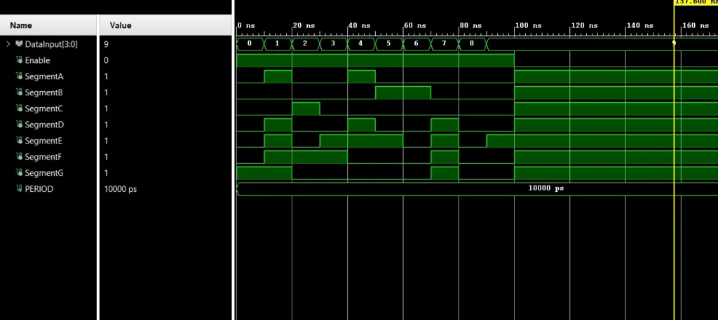
In this tutorial, we utilize 4-bit inputs, and the process only executes when receiving an active-high input. The 7-segment display operates based on the active-low statement.
The hexadecimal system can represent 16 different inputs, but in this context, we will only consider 10 input values because we can display values up to 9.
VHDL code for seven segment
library IEEE;
use IEEE.STD_LOGIC_1164.ALL;

entity SevenSegmentDisplay is
    Port (
        -- Inputs
        DataInput : in STD_LOGIC_VECTOR(3 downto 0);
        Enable : in STD_LOGIC;

        -- Outputs
        SegmentA, SegmentB, SegmentC, SegmentD, SegmentE, SegmentF, SegmentG : out STD_LOGIC
    );
end SevenSegmentDisplay;

architecture Behavioral of SevenSegmentDisplay is
    signal Segments : STD_LOGIC_VECTOR(6 downto 0);

begin
    process(DataInput, Enable)
    begin
        if Enable = '1' then  -- Active-high input
            case DataInput is
                when "0000" =>
                    Segments <= "0000001"; -- Display 0
                when "0001" =>
                    Segments <= "1001111"; -- Display 1
                when "0010" =>
                    Segments <= "0010010"; -- Display 2
                when "0011" =>
                    Segments <= "0000110"; -- Display 3
                when "0100" =>
                    Segments <= "1001100"; -- Display 4
                when "0101" =>
                    Segments <= "0100100"; -- Display 5
                when "0110" =>
                    Segments <= "0100000"; -- Display 6
                when "0111" =>
                    Segments <= "0001111"; -- Display 7
                when "1000" =>
                    Segments <= "0000000"; -- Display 8
                when "1001" =>
                    Segments <= "0000100"; -- Display 9
                when others =>
                    Segments <= "1111111"; -- Display blank (for invalid inputs)
            end case;
        else
            Segments <= "1111111";  -- Display blank when Enable is low (inactive)
        end if;
    end process;

    -- Assign the segments to the outputs
    SegmentA <= Segments(6);
    SegmentB <= Segments(5);
    SegmentC <= Segments(4);
    SegmentD <= Segments(3);
    SegmentE <= Segments(2);
    SegmentF <= Segments(1);
    SegmentG <= Segments(0);

end Behavioral;
After RTL analysis, this type of circuit diagram will be generated
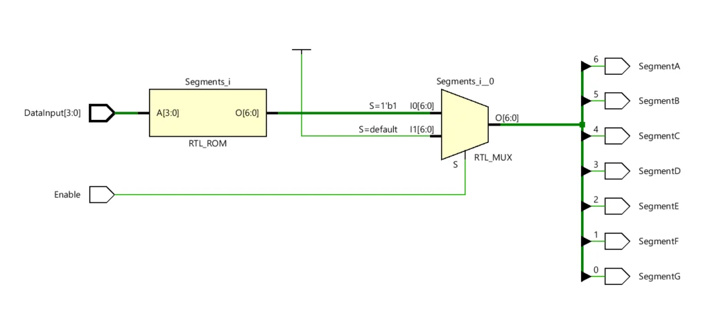
Actually, this is an intermediate component between 4-bit data input and a 7-segment display. We need to connect the 4 input wires properly and the 7-segment output wires properly.
Test bench
library IEEE;
use IEEE.STD_LOGIC_1164.ALL;

entity testbench_seven_segment_display is
end testbench_seven_segment_display;

architecture Behavioral of testbench_seven_segment_display is
    -- Constants
    constant PERIOD : time := 10 ns;

    -- Signals for the SevenSegmentDisplay entity
    signal DataInput : STD_LOGIC_VECTOR(3 downto 0) := "0000";
    signal Enable : STD_LOGIC := '0';
    signal SegmentA, SegmentB, SegmentC, SegmentD, SegmentE, SegmentF, SegmentG : STD_LOGIC;

    -- Component instantiation for SevenSegmentDisplay
    component SevenSegmentDisplay
        Port (
            -- Inputs
            DataInput : in STD_LOGIC_VECTOR(3 downto 0);
            Enable : in STD_LOGIC;

            -- Outputs
            SegmentA, SegmentB, SegmentC, SegmentD, SegmentE, SegmentF, SegmentG : out STD_LOGIC
        );
    end component;

begin
    -- DUT (Device Under Test) instantiation
    DUT: SevenSegmentDisplay
        port map (
            DataInput => DataInput,
            Enable => Enable,
            SegmentA => SegmentA,
            SegmentB => SegmentB,
            SegmentC => SegmentC,
            SegmentD => SegmentD,
            SegmentE => SegmentE,
            SegmentF => SegmentF,
            SegmentG => SegmentG
        );

    -- Stimulus process
    stim_proc: process
    begin
        -- Initialize signals (you can modify these values as needed)
        DataInput <= "0000";  -- Example value for DataInput (0 in binary)
        Enable <= '1';        -- Example value for Enable (active-high)

        wait for PERIOD;

        -- Change the values of DataInput to display other digits
        DataInput <= "0001";  -- Example value for DataInput (1 in binary)
        wait for PERIOD;
        DataInput <= "0010";  -- Example value for DataInput (2 in binary)
        wait for PERIOD;
        DataInput <= "0011";  -- Example value for DataInput (3 in binary)
        wait for PERIOD;
        DataInput <= "0100";  -- Example value for DataInput (4 in binary)
        wait for PERIOD;
        DataInput <= "0101";  -- Example value for DataInput (5 in binary)
        wait for PERIOD;
        DataInput <= "0110";  -- Example value for DataInput (6 in binary)
        wait for PERIOD;
        DataInput <= "0111";  -- Example value for DataInput (7 in binary)
        wait for PERIOD;
        DataInput <= "1000";  -- Example value for DataInput (8 in binary)
        wait for PERIOD;
        DataInput <= "1001";  -- Example value for DataInput (9 in binary)
        wait for PERIOD;

        -- Set Enable to low to turn off the display
        Enable <= '0';       -- Example value for Enable (inactive)

        wait;
    end process;
end Behavioral;
Simulation window
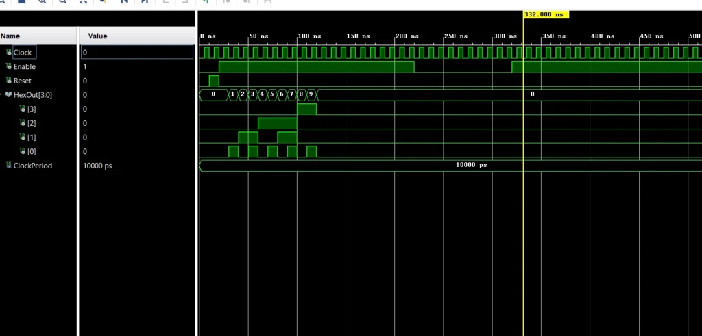
4.(VHDL tutorial 4.0)Design a Hexadecimal counter (0−F) with inputs
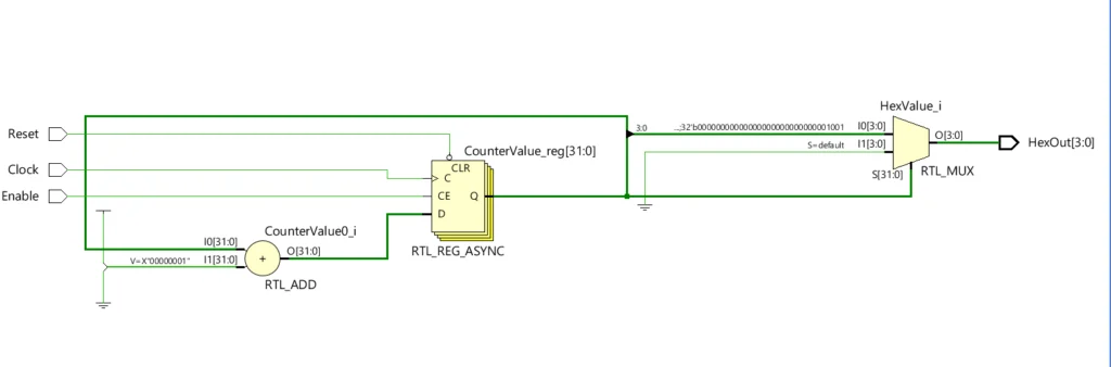
Basically, we have 3 inputs: Clock, Enable, and Reset. The counter has 4 outputs to give a hexadecimal output using 4 bits.
Clock: The Clock input serves as the main clock signal that controls the counting process. The counter will only increment its value when there is a rising edge (transition from ‘0’ to ‘1’) on this signal.
Reset (asynchronous): The Reset input is an asynchronous signal that allows us to reset the counter’s value to 0 immediately when it is asserted (pulled low), regardless of the clock’s state.
Enable: The Enable input controls whether the counter should increment or not. When the Enable signal is high (‘1’), the counter will increment on each rising edge of the Clock. When Enable is low (‘0’), the counter will remain at its last value.
Also we use “ieee.numeric_std.all” library for this VHDL tutorial.
uses of “ieee.numeric_std.all” library
- The program enables designers to precisely work with integers that have fractional parts using fixed-point and floating-point arithmetic. In VHDL, it aids in handling numbers like 3.14 (pi) or 2.5.
- The package includes types to represent numbers without or with a sign (positive or negative), as well as unsigned and signed kinds. When working with binary numbers like 1010 (10 in decimal) or 1111 (-1 in two’s complement), this is helpful.
- The package provides operations for working with unsigned and signed integers, such as addition, subtraction, multiplication, and division. This helps simple math procedures.
- Functions for comparison: This package includes functions for comparing numbers. For instance, you can determine whether one number is more than or less than another.
- routines for type conversion: This package contains routines for converting between various number types. For instance, you can change a decimal to a whole number or a whole number to a decimal.
- routines for Synchronization and Resolution: This package includes routines for managing various forms of data in VHDL. They ensure that data of all kinds can coexist without conflict.
- Code that can be synthesized: By using the package, you may be sure that the code can be implemented as hardware (such in a computer chip). For FPGA and ASIC designs, where hardware implementation is necessary, this is crucial.
- Keeping Away from Synthesis Pitfalls: The program is made to deal with unique situations and issues that may come up during hardware synthesis. It handles problems like dealing with overflowing numbers or unanticipated events.
VHDL main code
library IEEE;
use IEEE.STD_LOGIC_1164.ALL;
use IEEE.NUMERIC_STD.ALL;

entity HexadecimalCounter is
    Port (
        Clock   : in  STD_LOGIC;
        Enable  : in  STD_LOGIC;
        Reset   : in  STD_LOGIC;
        HexOut  : out STD_LOGIC_VECTOR(3 downto 0)
    );
end HexadecimalCounter;

architecture Behavioral of HexadecimalCounter is
    signal CounterValue : integer := 0;
begin
    process (Clock, Reset,Enable)
        variable HexValue : std_logic_vector(3 downto 0) := "0000";
    begin
        if Reset = '1' then
            CounterValue <= 0;  -- Asynchronous reset, set counter to 0
        elsif rising_edge(Clock) then
            if Enable = '1' then
                CounterValue <= CounterValue + 1;  -- Increment the counter when Enable is high
                report "CounterValue: " & integer'image(CounterValue);
            end if;
        end if;

        -- Convert the counter value to 4-bit hexadecimal representation
        case CounterValue is
            when 0 to 9 =>
                HexValue := std_logic_vector(to_unsigned(CounterValue, 4));
            when others =>
                HexValue := "0000";  -- Set to 0 for values greater than 9
        end case;

        -- Assign the 4-bit hexadecimal value to the output port
        HexOut <= HexValue;
    end process;
end Behavioral;
After RTL analysis, this type of circuit diagram will be generated
Test bench
library IEEE;
use IEEE.STD_LOGIC_1164.ALL;
use IEEE.NUMERIC_STD.ALL;

entity testbench_HexadecimalCounter is
end testbench_HexadecimalCounter;

architecture test of testbench_HexadecimalCounter is
    signal Clock, Enable, Reset : std_logic := '0';
    signal HexOut : std_logic_vector(3 downto 0);
    constant ClockPeriod : time := 10 ns;

    component HexadecimalCounter
        Port (
            Clock   : in  STD_LOGIC;
            Enable  : in  STD_LOGIC;
            Reset   : in  STD_LOGIC;
            HexOut  : out STD_LOGIC_VECTOR(3 downto 0)
        );
    end component;

begin
    -- Instantiate the DUT (Device Under Test)
    DUT: HexadecimalCounter
        Port Map (
            Clock => Clock,
            Enable => Enable,
            Reset => Reset,
            HexOut => HexOut
        );

    -- Clock generation process
    ClockProcess : process
    begin
        Clock <= '0';
        wait for ClockPeriod / 2;
        Clock <= '1';
        wait for ClockPeriod / 2;
    end process;

    -- Stimulus process
    StimulusProcess: process
    begin
        -- Asynchronous reset (initial state)
        Reset <= '0';
        Enable <= '0';
        wait for ClockPeriod;
        Reset <= '1';
        wait for ClockPeriod;
        Reset <= '0';

        -- Test with Enable = '1', expect counting from 0 to 9
        Enable <= '1';
        wait for ClockPeriod * 20; -- Run for 200 ns to observe the outputs

        -- Test with Enable = '0', expect counting stops at 9
        Enable <= '0';
        wait for ClockPeriod * 10;

        -- Test with Enable = '1', expect counting resumes from 0
        Enable <= '1';
        wait for ClockPeriod * 20; -- Run for 200 ns to observe the outputs

        wait;
    end process;
end test;
Simulation window
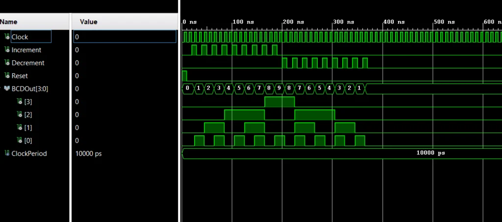
5.(VHDL tutorial 5.0)Design an Up/Down BCD counter (0−9) with inputs
BCD counter
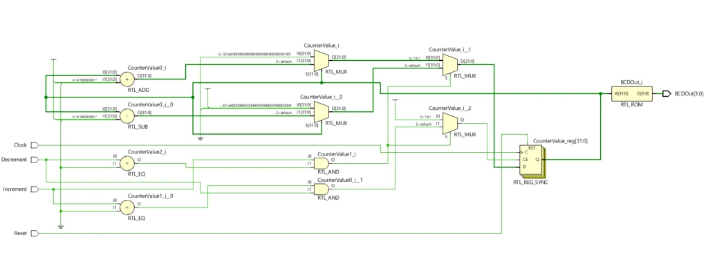
A BCD (Binary Coded Decimal) counter, also termed as a decade counter, is designed to count from 0 to 9 in binary representation. It takes two input lines, one for incrementing the count and another for decrementing it. The counter increments or decrements by 1 at a time, and the count is represented in 4-bit binary format since it covers values from 0 (0000) to 9 (1001). When the counter exceeds 9, it automatically resets to 0. Additionally, there is a reset input that allows us to manually reset the counter to 0 at any time. All the operations are synchronized with the clock signal.
Truth table
| Reset pin | Input | D | C | B | A |
| 0 | 0 | 0 | 0 | 0 | 0 |
| 0 | 1 | 0 | 0 | 0 | 1 |
| 0 | 2 | 0 | 0 | 1 | 0 |
| 0 | 3 | 0 | 0 | 1 | 1 |
| 0 | 4 | 0 | 1 | 0 | 0 |
| 0 | 5 | 0 | 1 | 0 | 1 |
| 0 | 6 | 0 | 1 | 1 | 0 |
| 0 | 7 | 0 | 1 | 1 | 1 |
| 0 | 8 | 1 | 0 | 0 | 0 |
| 0 | 9 | 1 | 0 | 0 | 1 |
| 0 | 10 | 0(RESET) | 0(RESET) | 0(RESET) | 0(RESET) |
VHDL code for bcd counter
library IEEE;
use IEEE.STD_LOGIC_1164.ALL;
use IEEE.NUMERIC_STD.ALL;

entity BCDCounter is
    Port (
        Clock      : in  STD_LOGIC;
        Increment  : in  STD_LOGIC;
        Decrement  : in  STD_LOGIC;
        Reset      : in  STD_LOGIC;
        BCDOut     : out STD_LOGIC_VECTOR(3 downto 0)
    );
end BCDCounter;

architecture Behavioral of BCDCounter is
    signal CounterValue : integer := 0;  -- Integer variable for the counter value (0 to 9)
begin
    process (Clock)
    begin
        if rising_edge(Clock) then
            if Reset = '1' then
                CounterValue <= 0;  -- Reset the counter to 0
            else
                if Increment = '1' and Decrement = '0' then
                    if CounterValue = 9 then
                        CounterValue <= 0; -- Reset the counter to 0 when it exceeds 9
                    else
                        CounterValue <= CounterValue + 1; -- Increment the counter by 1
                    end if;
                elsif Increment = '0' and Decrement = '1' then
                    if CounterValue = 0 then
                        CounterValue <= 9; -- Set the counter to 9 when decrementing from 0
                    else
                        CounterValue <= CounterValue - 1; -- Decrement the counter by 1
                    end if;
                end if;
            end if;
        end if;
    end process;

    -- Convert the 4-bit binary value to BCD (Binary Coded Decimal) representation
    process (CounterValue)
    begin
        case CounterValue is
            when 0 =>
                BCDOut <= "0000"; -- BCD representation of 0
            when 1 =>
                BCDOut <= "0001"; -- BCD representation of 1
            when 2 =>
                BCDOut <= "0010"; -- BCD representation of 2
            when 3 =>
                BCDOut <= "0011"; -- BCD representation of 3
            when 4 =>
                BCDOut <= "0100"; -- BCD representation of 4
            when 5 =>
                BCDOut <= "0101"; -- BCD representation of 5
            when 6 =>
                BCDOut <= "0110"; -- BCD representation of 6
            when 7 =>
                BCDOut <= "0111"; -- BCD representation of 7
            when 8 =>
                BCDOut <= "1000"; -- BCD representation of 8
            when 9 =>
                BCDOut <= "1001"; -- BCD representation of 9
            when others =>
                BCDOut <= "0000"; -- Set to 0 for invalid values
        end case;
    end process;
end Behavioral;
After RTL analysis, this type of circuit diagram will be generated
Test bench
library IEEE;
use IEEE.STD_LOGIC_1164.ALL;
use IEEE.NUMERIC_STD.ALL;

entity testbench_BCDCounter is
end testbench_BCDCounter;

architecture test of testbench_BCDCounter is
    signal Clock, Increment, Decrement, Reset : std_logic := '0';
    signal BCDOut : std_logic_vector(3 downto 0);
    constant ClockPeriod : time := 10 ns;

    component BCDCounter
        Port (
            Clock      : in  STD_LOGIC;
            Increment  : in  STD_LOGIC;
            Decrement  : in  STD_LOGIC;
            Reset      : in  STD_LOGIC;
            BCDOut     : out STD_LOGIC_VECTOR(3 downto 0)
        );
    end component;

begin
    -- Instantiate the DUT (Device Under Test)
    DUT: BCDCounter
        Port Map (
            Clock => Clock,
            Increment => Increment,
            Decrement => Decrement,
            Reset => Reset,
            BCDOut => BCDOut
        );

    -- Clock generation process
    ClockProcess : process
    begin
        Clock <= '0';
        wait for ClockPeriod / 2;
        Clock <= '1';
        wait for ClockPeriod / 2;
    end process;

    -- Stimulus process
    StimulusProcess: process
    begin
        -- Asynchronous reset (initial state)
        Reset <= '1';
        wait for ClockPeriod;
        Reset <= '0';
        wait for ClockPeriod;

        -- Test with Increment = '1', expect counting from 0 to 9
        Increment <= '1';
        wait for ClockPeriod ;
        Increment <= '0';
        wait for ClockPeriod ;
        Increment <= '1';
        wait for ClockPeriod ;
        Increment <= '0';
        wait for ClockPeriod ;
        Increment <= '1';
        wait for ClockPeriod ;
        Increment <= '0';
        wait for ClockPeriod ;
        Increment <= '1';
        wait for ClockPeriod ;
        Increment <= '0';
        wait for ClockPeriod ;
        Increment <= '1';
        wait for ClockPeriod ;
        Increment <= '0';
        wait for ClockPeriod ;
        Increment <= '1';
        wait for ClockPeriod ;
        Increment <= '0';
        wait for ClockPeriod ;
        Increment <= '1';
        wait for ClockPeriod ;
        Increment <= '0';
        wait for ClockPeriod ;
        Increment <= '1';
        wait for ClockPeriod ;
        Increment <= '0';
        wait for ClockPeriod ;
        Increment <= '1';
        wait for ClockPeriod ;
        Increment <= '0';
        wait for ClockPeriod ;

        -- Test with Decrement = '1', expect counting from 9 to 0
        Decrement <= '1';
        wait for ClockPeriod ;
        Decrement <= '0';
        wait for ClockPeriod ;
        Decrement <= '1';
        wait for ClockPeriod ;
        Decrement <= '0';
        wait for ClockPeriod ;
        Decrement <= '1';
        wait for ClockPeriod ;
        Decrement <= '0';
        wait for ClockPeriod ;
        Decrement <= '1';
        wait for ClockPeriod ;
        Decrement <= '0';
        wait for ClockPeriod ;
        Decrement <= '1';
        wait for ClockPeriod ;
        Decrement <= '0';
        wait for ClockPeriod ;
        Decrement <= '1';
        wait for ClockPeriod ;
        Decrement <= '0';
        wait for ClockPeriod ;
        Decrement <= '1';
        wait for ClockPeriod ;
        Decrement <= '0';
        wait for ClockPeriod ;
        Decrement <= '1';
        wait for ClockPeriod ;
        Decrement <= '0';
        wait for ClockPeriod ;
        Decrement <= '1';
        wait for ClockPeriod ;
        Decrement <= '0';
        wait for ClockPeriod ;

        wait;
    end process;
end test;
Simulation window
Read more about FPGA
helloI like your writing very so much proportion we keep up a correspondence extra approximately your post on AOL I need an expert in this space to unravel my problem May be that is you Taking a look forward to see you
[…] and VHDL are the primary hardware programming languages. Vivado serves as the software platform, comparable […]
Thank you for the good writeup It in fact was a amusement account it Look advanced to far added agreeable from you However how could we communicate
Thank you for the auspicious writeup It in fact was a amusement account it Look advanced to more added agreeable from you By the way how could we communicate
Hello i think that i saw you visited my weblog so i came to Return the favore Im trying to find things to improve my web siteI suppose its ok to use some of your ideas
Thank you for your sharing. I am worried that I lack creative ideas. It is your article that makes me full of hope. Thank you. But, I have a question, can you help me?
Fruit Party
実用性の高い情報で満足です。これからも期待しています。
Thanks for sharing. I read many of your blog posts, cool, your blog is very good.
What i do not understood is in truth how you are not actually a lot more smartlyliked than you may be now You are very intelligent You realize therefore significantly in the case of this topic produced me individually imagine it from numerous numerous angles Its like men and women dont seem to be fascinated until it is one thing to do with Woman gaga Your own stuffs nice All the time care for it up