
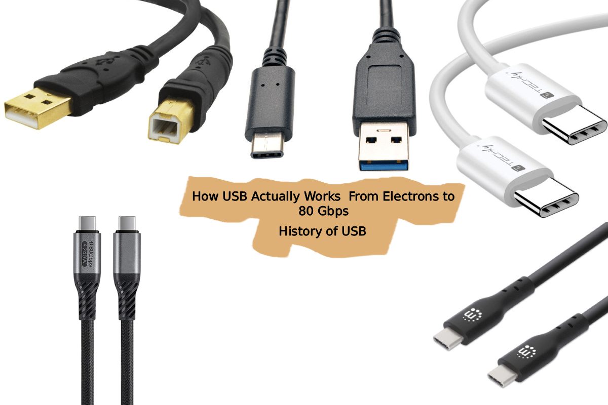
Every time you plug in a phone charger, copy files to a flash drive, or connect a keyboard, a tiny but deeply engineered system wakes up. That rectangular or oval port you take for granted has quietly gone through seven major generations since 1996, each time reinventing the physics of how electricity carries information. Let’s rip it open pin by pin, bit by bit.
Click to jump
- Why USB Even Exists: The Problem It Solved (Jump)
- The Chaos Before USB: Serial, Parallel, PS/2 and More
- Why “Serial” Beats “Parallel” at High Speed
- The Seven Founders and the Birth of USB 1.0
- How USB Sends a Bit: The Voltage Language (Jump)
- NRZI Encoding: No Changes Mean “1”, a Change Means “0”
- Bit Stuffing: Forcing Transitions to Keep the Clock Alive
- Differential Signaling: Why D+ and D− Cancel Out Noise
- The Generations: What Actually Changed Physically? (Jump)
- The Full Spec Table: 1996 to 2022
- USB 1.0 to 2.0 — Same Wires, Faster Transistors
- USB 3.0 — A Hidden Second Bus Inside the Same Plug
- 8b/10b Encoding and the DC Balance Problem
- LFSR Scrambling: Spectrum Engineering, Not Encryption
- Deep Dive #1 — The Physics of High-Speed Signaling: Why Speed Has a Distance Problem (Jump)
- When a Wire Stops Being a Wire: Transmission Line Theory
- Impedance Mismatches and Signal Reflections
- Why USB4 Cables Beyond 1 Meter Need Repeater Chips
- Deep Dive #2 — Inside the USB Controller Chip: Transistors Doing Three Jobs at Once (Jump)
- Job 1: Voltage Comparator — How USB-C Detects Orientation
- Job 2: High-Speed Line Driver — Why the Swing Drops at 5 Gbps
- Job 3: Digital Logic — The Protocol State Machine and CRC Math
- The USB Type-C Connector: 24 Pins, Infinite Flexibility (Jump)
- VBUS, GND, D+/D−: The Legacy Pins
- SSTX, SSRX, CC1/CC2: The SuperSpeed and Control Pins
- SBU1/SBU2: The Secret Behind DisplayPort Alternate Mode
- Deep Dive #3 — USB4 and the PAM3 Revolution: When Binary Is No Longer Enough (Jump)
- Why 80 Gbps Is Impossible with Binary Signaling on Real Cables
- PAM3: Three Voltage Levels, 1.58 Bits Per Symbol
- 11 Bits → 7 Trits: How USB4 v2.0 Packs More Into Less
- The Eye Diagram and Why Forward Error Correction Is Mandatory
- The Bigger Picture: Why Each Generation Needed New Physics (Jump)
- Seven Transitions, Seven Physics Walls
- From Transistor Speed to Modulation Theory: The Full Arc
Why USB Even Exists: The Problem It Solved
Before USB, your desktop computer had a chaotic collection of ports serial (COM), parallel (LPT), PS/2 for keyboards and mice, game ports for joysticks, and more. Each port used a different connector, a different voltage, a different protocol. Plugging in a printer was an event that sometimes required rebooting. The industry needed one universal standard, and in January 1996, seven companies Intel, Microsoft, IBM, NEC, Compaq, DEC, and Nortel published USB 1.0. The name itself says everything: Universal (works with everything), Serial (sends bits one at a time, not in parallel), Bus (a shared electrical highway that multiple devices can talk on).
The word “serial” is worth pausing on. A serial bus sends data as a single stream of bits one after another through one wire. A parallel bus sends multiple bits simultaneously across multiple wires. Parallel sounds faster, but at high frequencies, the tiny timing differences between wires (called skew) causes data corruption. Serial transmission sidesteps this entirely, which is why USB, PCIe, SATA, and virtually every modern high-speed interface is serial.
(back to menu)
How USB Sends a Bit: The Voltage Language
Before diving into generations, it is worth understanding the most fundamental question how does a USB cable actually carry a “1” or a “0”?
USB does not use a simple “high voltage = 1, low voltage = 0” scheme, because at high speeds a constant high or low voltage would cause the receiver to lose synchronization it cannot tell whether it is receiving ten “1”s or whether the wire is simply doing nothing. Instead, USB uses NRZI (Non-Return to Zero Invert) encoding: a “1” is represented by no change in voltage level, while a “0” is represented by a change in voltage level. This way, a long stream of zeros still toggles the line repeatedly, keeping the receiver’s clock locked in.
But what if the data happens to be a long string of ones? No transitions would occur, and the receiver would drift out of sync. USB solves this with bit stuffing: a forced “0” bit is inserted into the data stream after every six consecutive “1”s. The receiver knows this rule and strips out those inserted bits. The result is that the line always transitions at least once every seven bits the receiver can always find the beat.
Additionally, USB uses differential signaling: it sends every bit on two wires simultaneously, called D+ and D−, with opposite voltages. The receiver measures only the difference between D+ and D−, not the absolute voltage. Any electrical noise affects both wires equally, so the difference cancels it out this is the physics behind USB’s remarkable noise immunity, and it is the same principle used in professional audio and in modern fiber-optic transmitters.
(back to menu)
The Generations: What Actually Changed Physically?
The spec table below summarizes the journey, but what matters is why each jump happened and the answer is always a combination of electronics engineering and clever physics.
(back to menu)
USB 1.0 to 2.0 Same Wires, Faster Transistors
USB 1.0’s maximum speed of 12 Mbps was limited by the switching speed of the transistors inside the controller chip’s physical layer (PHY). The PHY is the block of circuitry responsible for turning digital 1s and 0s into actual voltage pulses on the cable. USB 2.0, released in April 2000, kept the exact same four-pin connector (one VBUS power, one GND, D+, D−) but upgraded the PHY transistors to switch 40× faster, achieving 480 Mbps. No new wires were needed the bottleneck was purely in silicon speed, not in the cable.
USB 3.0 A Hidden Second Bus Inside the Same Plug
USB 3.0 is the most architecturally dramatic shift. Instead of speeding up the original D+/D− pair, engineers added an entirely second signaling system inside the same connector. A USB 3.0 Type-A connector has 9 pins (versus 4 in USB 2.0): the original 4 pins are retained for backward compatibility, and 5 new pins are added one pair for SuperSpeed transmit (SSTX+/−), one pair for SuperSpeed receive (SSRX+/−), and one ground. This means USB 3.0 is full-duplex at SuperSpeed: it can send and receive simultaneously through dedicated lanes, unlike USB 2.0 which shared one pair for both directions (half-duplex).
At 5 Gbps, the signal changes voltage 5 billion times per second. At these frequencies, the raw NRZ signal would have too much DC bias the average voltage would drift, confusing the receiver’s amplifiers. USB 3.0 therefore introduced 8b/10b encoding: every 8-bit data byte is translated into a 10-bit symbol chosen from a table that guarantees the symbol contains roughly equal numbers of 0s and 1s, keeping the average voltage balanced (this is called DC balance). The downside is a 20% overhead for every 10 bits transmitted, only 8 carry actual data. That is why USB 3.0’s effective data throughput is about 400 MB/s, not the raw 500 MB/s its 5 Gbps line rate implies.
The USB 3.0 SuperSpeed data stream is also scrambled using a free-running Linear Feedback Shift Register (LFSR) before transmission. This is not encryption it is spectrum engineering. A repeating data pattern would concentrate radio emissions at specific frequencies, causing electromagnetic interference (EMI). Scrambling randomizes the energy across a broad spectrum so the cable does not act like a tiny antenna broadcasting on one frequency.
(back to menu)
Deep Dive #1: The Physics of High-Speed Signaling Why Speed Has a Distance Problem
This is one of the most physically fascinating aspects of USB that almost nobody talks about. Why can a USB 3.0 cable be at most 2 meters for passive operation, while a USB 2.0 cable can be 5 meters? The answer is rooted in high-frequency signal physics.
At low frequencies (USB 1.0/2.0), a wire is simply a wire electrons travel through it, and the voltage at the far end looks essentially the same as at the near end. At high frequencies (USB 3.0’s 2.5 GHz signal frequencies and above), a wire behaves as a transmission line, and the signal’s wavelength becomes comparable to the cable’s physical length. Under these conditions, signals partially reflect at impedance mismatches (connectors, joints, the socket itself), and the reflected wave travels back and interferes with the forward wave causing what is called signal integrity degradation.
USB 3.0 cables therefore require tightly controlled twisted-pair differential wiring: the two wires of each SS pair are twisted together at a specified rate, which keeps their impedance matched and cancels magnetic interference. USB 3.2 Gen 2×2 (20 Gbps) reduces the passive cable limit to about 1 meter, because the signal now toggles at 5 GHz any longer and the reflections corrupt the data. This is why USB4 and Thunderbolt 4 cables beyond 1 meter are active cables they contain small repeater chips inside the connector housing that regenerate and re-time the signal, burning milliwatts of power to overcome physics.
(back to menu)
Deep Dive #2: Inside the USB Controller Chip Transistors Doing Three Jobs at Once
When you plug a USB device in, a controller chip on both ends springs to life. This chip called the USB PHY (Physical Layer Transceiver) is a complex piece of mixed-signal silicon that performs three distinct jobs simultaneously using transistors in three different modes.
Job 1 Voltage Comparator (Transistors as Sensors). The moment a cable is inserted, the PHY’s transistors operate in their linear amplification mode to detect the voltage state on the CC (Configuration Channel) pin a special pin present in USB-C that did not exist in older connectors. The voltage on CC is set by pull-up or pull-down resistors, and the PHY reads whether CC is high or low. If CC1 is high and CC2 is low, the chip knows the cable is inserted “right-side up.” If CC1 is low and CC2 is high, it is upside down. In either case, the internal routing multiplexers (made of transmission-gate transistors) flip the signal paths accordingly that is why USB-C is reversible.
Job 2 High-Speed Switch (Transistors as Line Drivers). During actual data transmission, the PHY’s output-stage transistors operate as ultra-fast switches to drive the D+/D− or SSTX+/SSTX− lines. In USB 2.0, the transistors switch between 0 V and 3.3 V (and specific termination voltages) at 480 million times per second. In USB 3.0, the output swing is actually reduced to around 800 mV differential, because at 5 Gbps the transistors simply cannot slew a full 3.3 V swing fast enough. Lower swing means faster switching, at the cost of reduced noise margin which is why the cable quality requirements become stricter.
Job 3 Digital Logic (Transistors as Arithmetic Units). Behind the PHY is the USB link layer controller a digital CMOS block where billions of transistors implement the USB protocol state machine. This logic handles the USB packet structure (SOF tokens, SETUP packets, DATA packets, ACK/NAK handshakes), the CRC error detection math, and the power negotiation messaging. The Texas Instruments TUSB1310 USB 3.0 PHY, for example, runs its digital PIPE interface at 250 MHz with 16-bit SDR mode to feed the link layer meaning 4 billion bits per second flow between the PHY silicon and the link controller on-chip.
(back to menu)
The USB Type-C Connector: 24 Pins, Infinite Flexibility
USB Type-C, standardized in 2014, is not a new speed it is a new connector that can carry multiple protocols. Its 24 pins serve five distinct functions:
- VBUS × 4 Four power pins carry up to 5 A at 20 V (100 W, or 240 W under USB PD 3.1’s Extended Power Range)
- GND × 4 Four ground return paths handle the high current without the resistance of a single pin
- D+ / D− The original USB 2.0 single differential pair, preserved for backward compatibility with USB 2.0 devices
- SSTX1/2 and SSRX1/2 Two SuperSpeed transmit pairs and two SuperSpeed receive pairs, duplicated for both cable orientations
- CC1 and CC2 The Configuration Channel pins, used for orientation detection, power negotiation messages, and Alternate Mode switching
- SBU1 and SBU2 Sideband Use pins, which carry non-USB signals in Alternate Mode for example, DisplayPort audio or video data when the connector is reconfigured as a DisplayPort output
The SBU pins are particularly clever. When DisplayPort Alternate Mode is active, the USB-C connector physically repurposes two of its SuperSpeed lanes and both SBU wires to carry DisplayPort signals, while the USB 2.0 D+/D− pair continues to carry USB data simultaneously. The connector is not just a connector it is a configurable switch fabric made of metal contacts and firmware logic.
(back to menu)
Deep Dive #3: USB4 and the PAM3 Revolution When Binary Is No Longer Enough
USB4 v2.0 (2022) achieves 80 Gbps a figure that is physically impossible to reach by simply making transistors switch faster on existing USB-C cables. Here is why, and how they solved it.
At USB4 Gen 3 (40 Gbps), the signal on each lane toggles at 20 GHz. The USB-C cables already in circulation cannot cleanly transmit signals much beyond that frequency signal loss in the cable (called insertion loss) increases steeply with frequency, and the signal arrives at the far end attenuated and distorted. To double to 80 Gbps without doubling the frequency, USB4 v2.0 introduced a fundamentally different modulation scheme: PAM3 (Pulse Amplitude Modulation, 3-level).
In traditional binary (NRZ/PAM2) signaling, each symbol carries exactly 1 bit the voltage is either high (1) or low (0). PAM3 uses three voltage levels: +1, 0, and −1. With three states, each symbol encodes log23≈1.58 bits of information. USB4 v2.0 formalizes this by mapping 11 binary bits into 7 “trits” (base-3 symbols) for transmission. Each lane runs at 25.6 GBaud (25.6 billion symbols per second), but since each symbol carries more than 1 bit, the effective data rate per lane exceeds 40 Gbps yielding 80 Gbps across two lanes. This is the same philosophy behind 5G NR modulation and modern optical communications: squeeze more bits per symbol rather than increasing the symbol rate.
The PAM3 receiver is significantly more demanding than a binary receiver. Instead of comparing one voltage threshold (“is it above or below 0.4 V?”), the receiver must distinguish two thresholds simultaneously (“is it in the top third, middle third, or bottom third of the voltage range?”). The eye diagram a standard oscilloscope view used by hardware engineers to assess signal quality shows two distinct “eyes” stacked vertically instead of one, and both must remain open under all temperature and interference conditions. This is why USB4 v2.0 specification demands forward error correction (FEC) on the link: at PAM3 speeds, the bit error rate without FEC would be unacceptably high for reliable data transfer.
(back to menu)
The Bigger Picture: Why Each Generation Needed New Physics
Looking across all seven generations, a clear pattern emerges. Each generation hit a wall not a software wall, but a physics wall and engineers had to invent new techniques to break through it:
- USB 1.0 → 2.0: The wall was transistor switching speed. Breaking it required faster CMOS fabrication processes for the PHY chip.
- USB 2.0 → 3.0: The wall was the D+/D− pair’s bandwidth ceiling. Breaking it required adding entirely new wire pairs inside the cable and inventing 8b/10b DC-balanced encoding.
- USB 3.0 → 3.1: The wall was the 20% encoding overhead of 8b/10b. Breaking it required switching to 128b/132b encoding, dropping overhead from 20% to just 3%.
- USB 3.1 → 3.2: The wall was single-lane frequency limits. Breaking it required running two lanes simultaneously, doubling bandwidth without increasing per-lane frequency.
- USB 3.2 → USB4: The wall was proprietary fragmentation (Thunderbolt vs. USB). Breaking it required Intel donating the Thunderbolt 3 protocol to the USB-IF, merging both ecosystems.
- USB4 → USB4 v2.0: The wall was binary modulation’s spectral efficiency. Breaking it required switching from 2-level to 3-level (PAM3) signaling a fundamental change in how voltage encodes information.
Every time the speed doubled, it was not because engineers found a shortcut. It was because they went deeper into physics into encoding theory, transmission line behavior, or modulation mathematics and found a new way to make the same copper wires carry more information. The port you plug your phone into every night is, quietly, one of the most elegant demonstrations of applied physics in everyday life.
From a 12 Mbps serial bus born in 1996 to an 80 Gbps PAM3 signaling standard in 2022, USB’s entire history is the story of engineers repeatedly answering the same question “how do you make electricity talk faster?” with a new answer each time.
(back to menu)
Read more – https://circuitprofessor.com/category/circuitprofessor-explanations/