PCB stands for Printed Circuit Board, and this article will provide all the steps along with external tips and tricks.
In this article, we discuss the following subtopics.
- Understanding the theory while discovering the optimal method in PCB.(click)
- Create a schematic while exploring the availability and feasibility of weather-seeking devices. (click)
- Simulating the project.(click)
- Purchased devices and conducted a trial using a breadboard. (click)
- draw a PCB design(click)
- File exporting(click)
- Frequently Asked Questions (FAQs)(click)
1. Understanding the theory while discovering the optimal method.
First, you need to find the optimal solution from all possible solutions.
For example, if you need to create a voltage controller circuit for a motor, you can change the voltage by using a variable resistor, PWM signals, or a resistor circuit. Then, identify whether that solution is feasible or not, as in the case of PWM signals. Research your chosen solution and explore alternative solutions, such as the best way to generate PWM signals and how to use those PWM signals to change voltage.
Then, identify the requirements, which means whether you want to change the voltage in small segments or if precise changes are unnecessary. Next, identify your inputs and outputs.
2. Create a schematic while exploring the availability and feasibility of weather-seeking devices.
Then, you have to consider component availability while designing the schematics. otherwise, you can’t complete your project. digiKey is the best site to find out the components. (If you are using EasyEDA, you can find built-in stores). Also, primarily consider 5 areas. Choosing components involves selecting various types of diodes, transistors, and resistors to fulfill specific tasks, power management, thermal management, Electromagnetic Compatibility (EMC), and Design for Manufacturability (DFM).
Mainly, these 3 are the best software options for drawing schematics: Altium Designer, EdrawMax, and Proteus.
3. Simulating the project.
Finally, it’s better to simulate your PCB design before creating a real-life implementation. You can analyze input and output from simulations, verify circuit behavior, and finally optimize design. The Proteus has good simulation capabilities.
4. Purchased devices and conducted a trial using a breadboard.
If you are going to fabricate this PCB yourself, then you need to first check your components. now that you have completed the computer simulation, proceed with the following steps: acquire all the necessary equipment and construct the circuit on a breadboard. Subsequently, verify the functionality of your circuit in a physical environment. (Note: Attach only the equipment that you intend to connect to your PCB.)
5. Draw a PCB design
This is the key point of the article. First, you need to find better software to draw your design. Mainly, 5 PCB designs are famous( Altium Designer, KiCad EDA, EasyEDA, Upverter, DipTrace, LibrePCB, and Fusion 360/Eagle).
1. Get all components to the window
First, you open your schematic design and PCB design software in separate windows. Next, you place all the components where you want them on your workspace.
Mainly, there are two types of PCB components: Through-Hole Technology (THT) and Surface-Mount Technology (SMT). In THT, components pass through the board, and these devices can be soldered from either the top or bottom layer. However, in SMT (Surface-Mount Devices (SMD)), components are mounted only on the surface. Therefore, soldering is done exclusively on the mounting surface. The main advantages of SMD include the absence of connections through the top and bottom layers.
Sometimes, you might not have the necessary files for the component footprint and device model to create the circuit. In this situation, you have two options. either add an external library to the software or create new files for the footprint and device.
2. Connection
Then, you must establish connections according to your schematics. It is simpler for you to create separate sections for circuits in your PCB design.
(This is a circuit diagram for a voltage controller using PWM signals.)
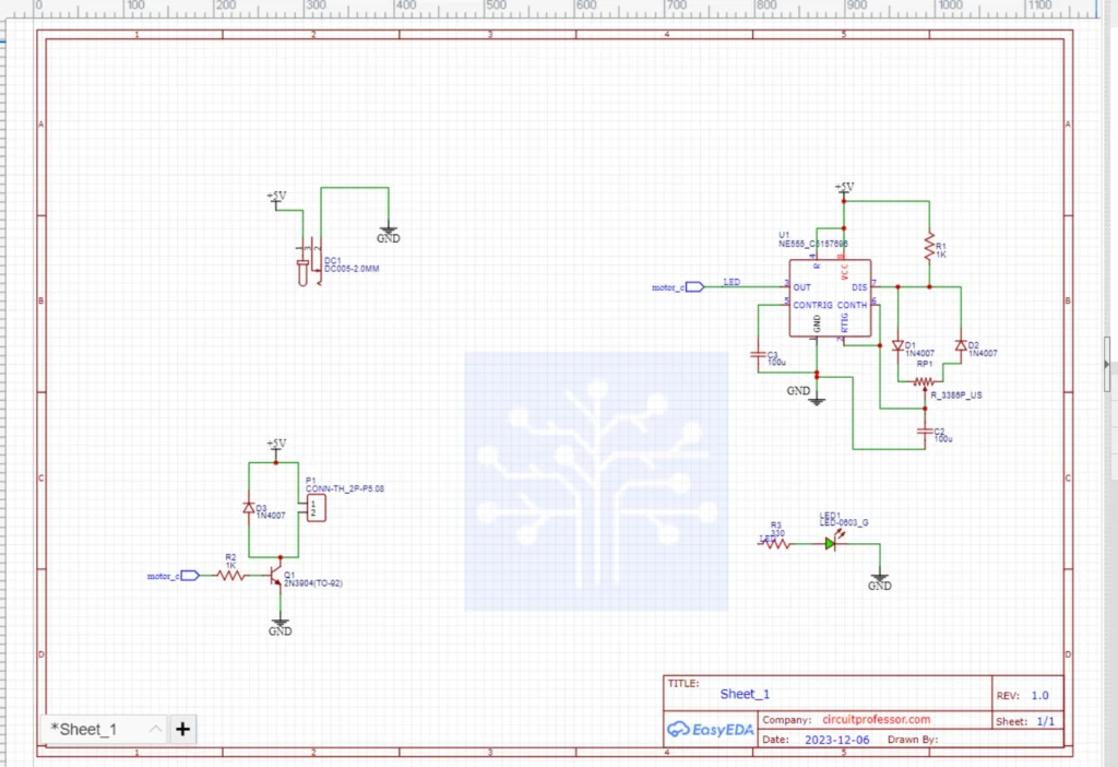
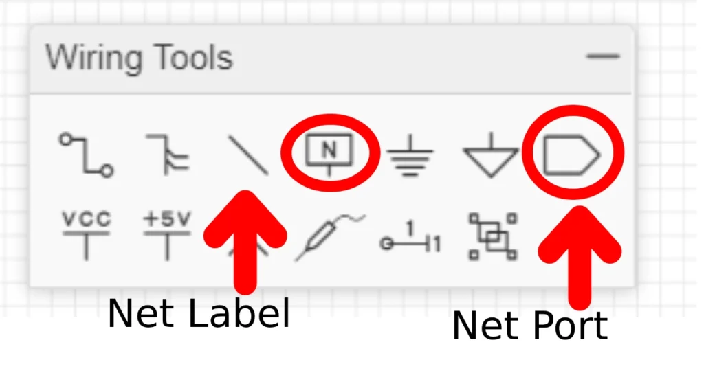
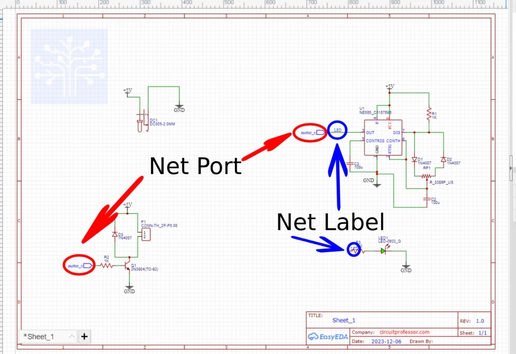
In this separate circuit, the GND and VCC (+5V) are the same for each one. All GND and VCC connections occur automatically on the PCB. Additionally, sometimes nodes located in each circuit connect. There are two methods for connecting separate circuits. (Net Label and Net Port).
First, save your design, and then proceed to convert it to PCB design.

3. Routing
Your PCB design windows will look like this. (Note: I use esayEDA )
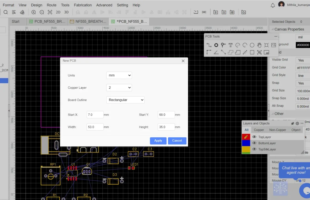
You can change the number of layers and adjust the dimensions of the PCB design. Click ‘OK’ to restore default settings.
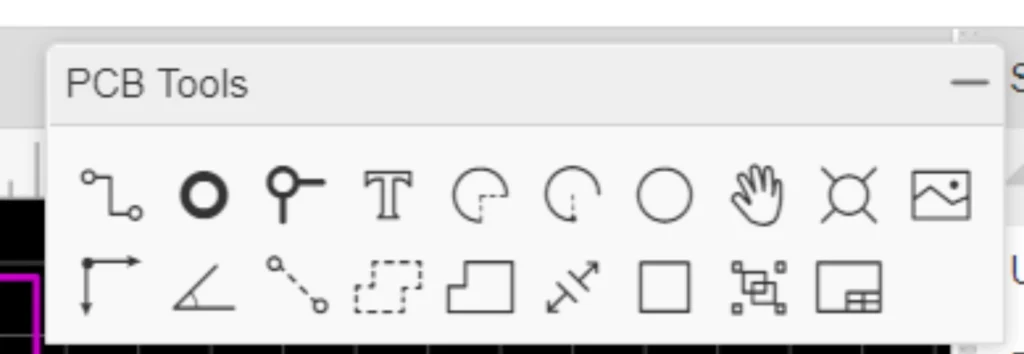
These tools comprise your toolbox for PCB design software.
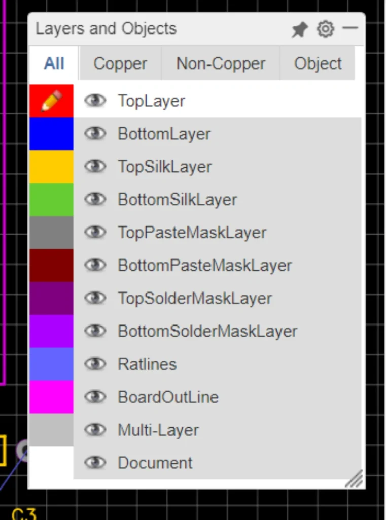
This is the layer box.
As a first step, you can remove the default boundary of the PCB design. After completing the entire design, you can recreate your boundary.
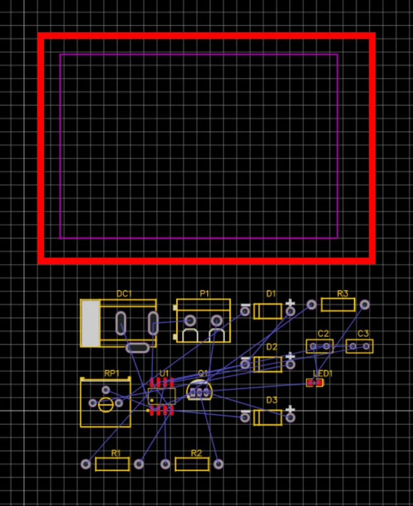
Cluster your components according to your previous circuit diagram because we need to simplify our design. Avoid crossing connection lines between components. You can rotate your components by pressing the SPACE bar.
Your final designs will look like this. You can change the component attachment to either the top or bottom layers.
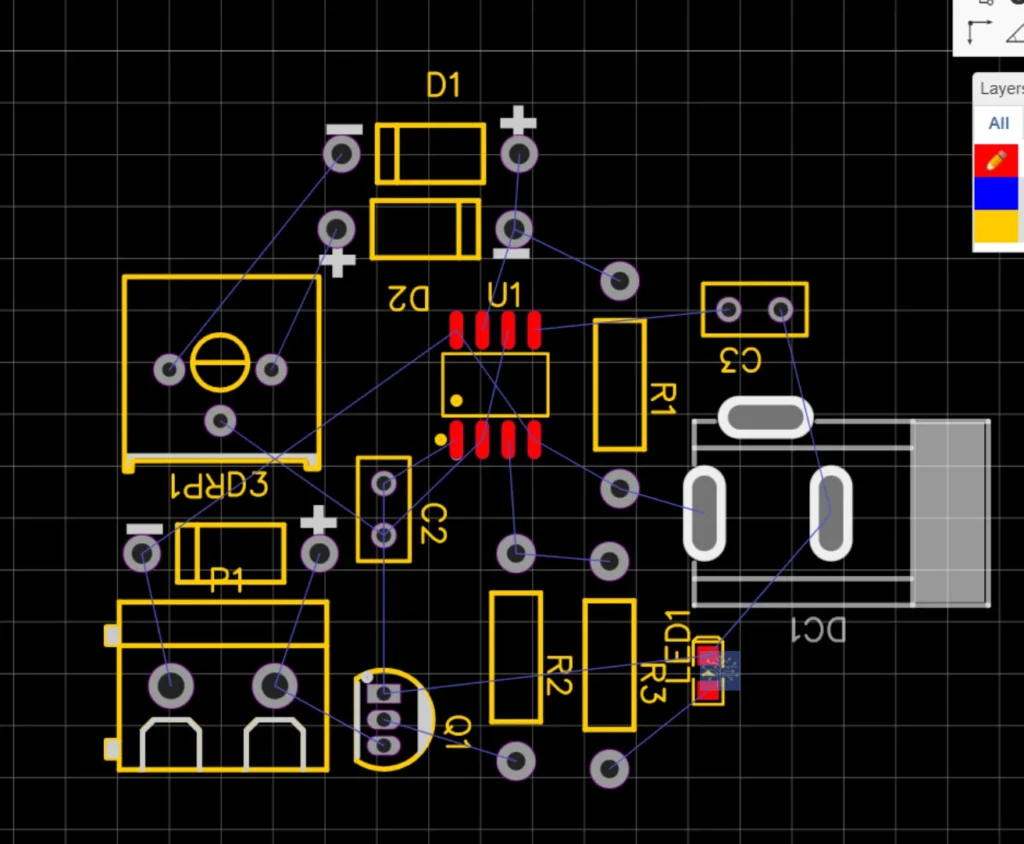
Finally, you can create boundaries using the “Track” tool. You can change the view of the design.

In this step, you can utilize the auto-routing option or manually route your PCB.
Routing path width
You can change the routing path width from here. When you are using high currents, it is better to use wider paths.
- To manage current flow in PCB traces:
- For thicker traces carrying 400mA, consider using the PCB Trace Width Calculators like (Saturn PCB Design Toolkit).
- Keep other traces under 30mA.
- Fast and inexpensive PCB fabricators typically have a minimum trace width of 5 or 6 mils.
- For high-tech boards, especially in military applications, trace widths can go as small as 2.5 mils or even smaller.
Routing strategy
Use of Via(V)
You can use vias to create connections between the top and bottom layers. These are essentially holes that go through the board. There are two purposes for using vias. Surface mount devices can be connected to other layers using vias, and to avoid cross-connections, we use vias.

The green square shows the Via, and you must change the Net name of the pin to match the Via. Then, the connection will be drawn automatically. By pressing “L,” you can change path angles. Sometimes, we will have to draw paths on other layers, such as the top and bottom layers.
Common layers
Most of the time, all the components’ ground layers are connected to the common copper zone layer.
Before the common copper layer
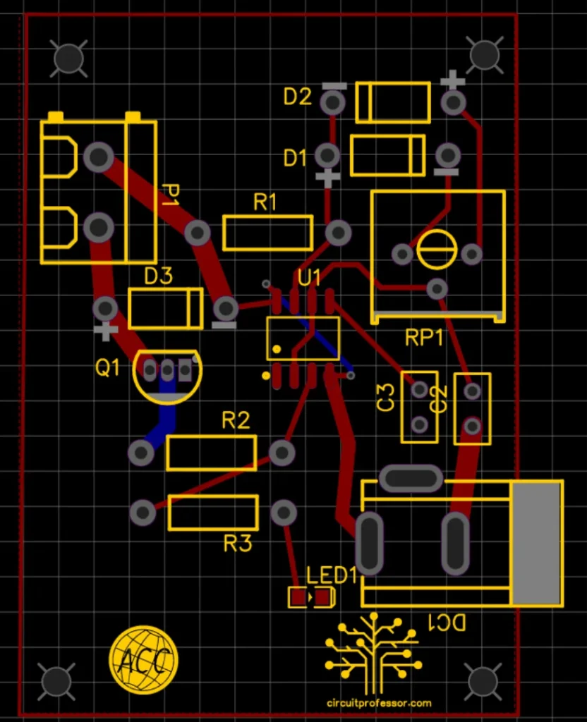
After the common copper layer

Clearance
Clearance refers to the gap between the common plane and the internal path.
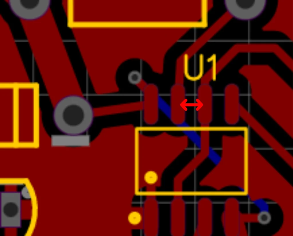
DRC(Design rule check)
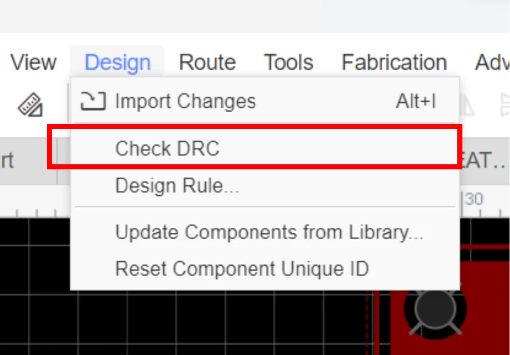
You can check whether the circuit has errors or not.
Then your final design looks like this.
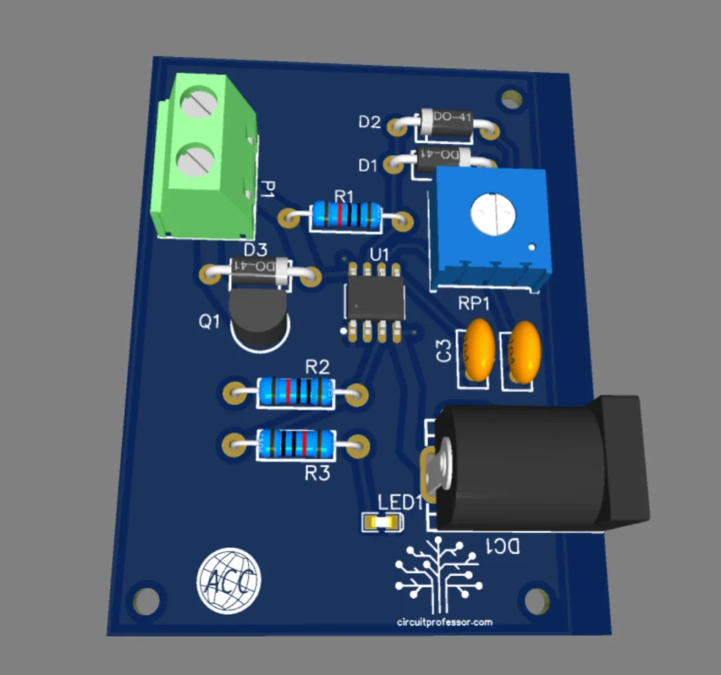
6. File exporting
In this section, we need to consider exporting files. In the normal PCB design process, we want to send Gerber and NC Drill Files. If you want to fabricate all the components on the PCB, then you have to send additional files such as the Bill of Materials (BOM), Pick-and-Place File, and Paste Mask File.
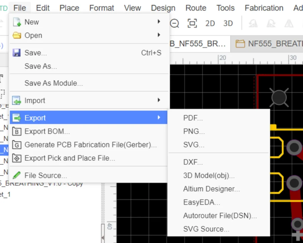
If you want to create your PCB from your location at a low cost, utilize the “Iron method.” You will need a PDF file to print the design. (Note that if your copper lines are only on the bottom layer, it is acceptable to take a normal print and paste it on the board. However, if your PCB has top copper layers, you must obtain a mirror image of the PCB design.)
In modern times, all PCBs are printed using machines. like V-One
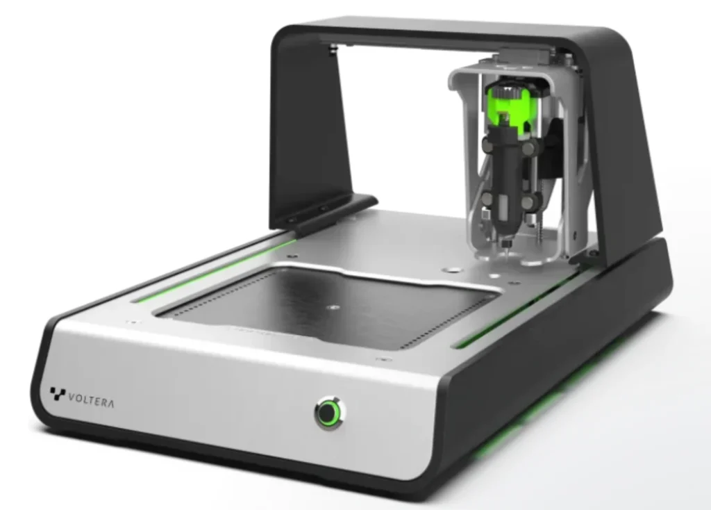
Atidiinatyy you can do a price comparison from this site – PCBShopper
In this article, you will receive a comprehensive A-to-Z explanation of PCB designs.
7. Frequently Asked Questions (FAQs)
- High-frequency wiring -When wiring digital high-frequency signals, take into account differential lines, space isolation, and impedance matching.
- Dense Wiring – To enhance electrical performance for high-frequency communications, reduce the number of vias, and take into account multi-layer boards.
- Decoupling Capacitors – To filter out stray signals, add them to the power supply port of your analog device at the right value.
- Reasonable layout, adequate power line redundancy, high-frequency impedance, and straightforward low-frequency wiring are characteristics of a good board.

This information is magnificent. I understand and respect your clear-cut points. I am impressed with your writing style and how well you express your thoughts.
This is a excellent blog, would you be involved in doing an interview about just how you designed it? If so e-mail me!
I like this blog so much, saved to my bookmarks .
If conceivable, as you clear knowledge, would you mind updating your blog with more information? It is damned helpful in return me.
Magnificent beat ! I would like to apprentice even as you amend your website,
how could i subscribe for a weblog website?
The account aided me a applicable deal. I had
been a little bit acquainted of this your broadcast provided vivid clear idea
Normally I do not read article on blogs however I would like to say that this writeup very forced me to try and do so Your writing style has been amazed me Thanks quite great post
hiI like your writing so much share we be in contact more approximately your article on AOL I need a specialist in this area to resolve my problem Maybe that is you Looking ahead to see you
Nice blog here Also your site loads up very fast What host are you using Can I get your affiliate link to your host I wish my site loaded up as quickly as yours lol
I loved as much as youll receive carried out right here The sketch is attractive your authored material stylish nonetheless you command get bought an nervousness over that you wish be delivering the following unwell unquestionably come more formerly again as exactly the same nearly a lot often inside case you shield this hike
helloI really like your writing so a lot share we keep up a correspondence extra approximately your post on AOL I need an expert in this house to unravel my problem May be that is you Taking a look ahead to see you
I抦 not sure where you are getting your information, but great topic. I needs to spend some time learning much more or understanding more. Thanks for great information I was looking for this information for my mission.
By doing so, education can equip students with the skills and adaptability needed to thrive in a world of constant change.
Incredible! This blog looks just like my old one! It’s on a entirely different
subject but it has pretty much the same page layout and design. Excellent choice of colors!
Its like you read my thoughts! You seem to grasp
so much approximately this, like you wrote the ebook in it or
something. I feel that you simply could do with some
p.c. to drive the message house a little bit,
however instead of that, this is wonderful blog.
A great read. I will definitely be back.
It’s a shame you don’t have a donate button! I’d most
certainly donate to this excellent blog! I suppose for now i’ll settle for book-marking and adding your RSS feed to my Google account.
I look forward to new updates and will share this website with my Facebook group.
Talk soon!
Wow! Thank you! I always wanted to write on my blog something like that. Can I implement a part of your post to my website?
I was suggested this web site by my cousin Im not sure whether this post is written by him as no one else know such detailed about my trouble You are incredible Thanks
Excellent blog here! Also your web site loads up very fast! What host are you using? Can I get your affiliate link to your host? I wish my web site loaded up as fast as yours lol