

The Mac Mini M4 is Apple’s most compact desktop computer, powered by a chip built at the 3-nanometer scale a scale so small that the transistors inside it are narrower than a strand of DNA. Sitting beneath it, the Ugreen 11-in-1 USB-C docking station quietly extends all that power into eleven physical ports. Together, this duo raises questions that go far deeper than spec sheets: How does a chip get built at 3nm? What actually moves data at 10 gigabits per second through a USB cable? Why is aluminum used instead of plastic? The answers pull you into some of the most fascinating corners of modern physics and electronics.
What Is This Combo, Exactly? (Mac Mini M4 + Ugreen 11-in-1 Hub)
The Apple Mac Mini (2024, M4) is a palm-sized desktop computer measuring just 12.7 × 12.7 × 5 cm and weighing about 670 grams. It ships with an Apple M4 SoC (System-on-Chip) that integrates a CPU, GPU, Neural Processing Unit, Digital Signal Processor, and memory all on a single die. Out of the box, it provides two USB-C ports (Thunderbolt 4) and three USB-A ports on the rear but the front face is completely bare.

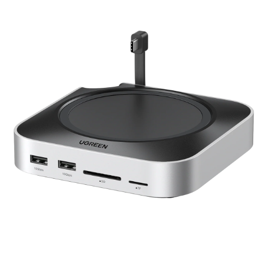
The Ugreen CM841 11-in-1 Docking Station is designed to sit directly underneath the Mac Mini, physically and functionally acting as a basement extension. It adds 3× USB-A 3.2 (10 Gbps), 2× USB-A 3.0 (5 Gbps), 2× USB-C 3.2 (10 Gbps), SD and TF card slots (104 MB/s), all in a body made from aluminum alloy and PVC, weighing 250g. The dock connects to the Mac Mini via a short ~4 cm USB-C host cable, which is precisely why it can sit flush underneath without any dangling wires.
Inside the M4 Chip: 28 Billion Transistors on 3nm
This is where the story becomes genuinely extraordinary. The M4 chip contains exactly 28 billion transistors that’s a 12% increase over the M3’s 25 billion all crammed onto a die fabricated using TSMC’s N3E second-generation 3-nanometer process. To put that in perspective: if you laid every transistor in this chip end to end, the line would stretch roughly 84,000 kilometres more than twice around the Earth.
What “3nm” Actually Means
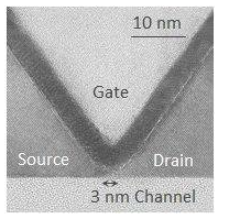
image – https://phys.org/news/2013-02-success-transistor-channel-length-nm.html
The “3nm” label doesn’t mean every feature is literally 3 nanometers wide. It is a node designation a marketing and classification name for a generation of manufacturing density. The real metric is transistor density, and TSMC’s N3E achieves a 1.6× higher logic transistor density compared to the older 5nm (N5) node, while offering 10–15% higher performance at the same power, or 30–35% lower power at the same performance. Three things make this possible: FinFET transistor architecture, Extreme Ultraviolet (EUV) lithography, and a design technique called FinFLEX.
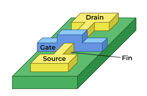
The FinFET Transistor: A 3D Switch
source and read more – https://www.geeksforgeeks.org/electronics-engineering/finfet/
A transistor is fundamentally a switch: it has three terminals a Source, a Drain, and a Gate and the Gate controls whether current can flow from Source to Drain. In the M4, this switch role is the primary function: billions of these transistors turn on and off billions of times per second, encoding binary logic (0 and 1) through their open and closed states. The secondary function is amplification of signal strength within the chip’s internal buses, ensuring signal integrity as electrical pulses travel between functional blocks.
What makes a FinFET special is its three-dimensional gate geometry. In older planar transistors, the gate sat flat on top of the channel like a flat lid it could only control current from one side, causing leakage as channels shrank. The FinFET wraps the gate around a thin, vertical fin of silicon on three sides (top + two sidewalls), giving it far more electrostatic control over the channel. The result? Leakage current drops dramatically, and the transistor can be turned on and off much more sharply which is exactly what you need when you’re packing 28 billion of them into a chip the size of a fingernail.
The TSMC N3E node also introduces FinFLEX technology, which allows chip designers to mix cells with different numbers of fins 1-fin, 2-fin, or 3-fin configurations on the same chip. A single-fin cell is more power-efficient; a triple-fin cell is faster. Engineers map the 4 “performance cores” of the M4’s CPU (which clock up to 4.4 GHz) onto high-fin, high-speed cells, while the 6 “efficiency cores” use low-fin, low-power cells. One chip, two personalities, optimized in silicon.
EUV Lithography: Writing With Light Shorter Than an Atom
How do you physically draw features that are only a few nanometers wide onto a silicon wafer? The answer is Extreme Ultraviolet Lithography (EUV), a process that uses light with a wavelength of 13.5 nanometers roughly 14× shorter than the deep-UV (193 nm) light used in older chipmaking. Shorter wavelength means finer resolution, just as a finer brush paints finer detail.
The process works in three physical stages. First, a tin (Sn) droplet about 30 micrometres in diameter is fired into a vacuum chamber and struck twice by an infrared laser: once to flatten it into a disc, and a second powerful pulse to vaporize it into a superheated plasma. This plasma emits EUV photons at 13.5 nm. Second, those photons are reflected and focused through a series of multilayer mirrors (since no lens material can transmit EUV without absorbing it) and projected through a photomask essentially a stencil of the circuit pattern onto a silicon wafer coated with a photosensitive material called a photoresist. Third, where the EUV light hits, it ionizes the photoresist, producing acids that chemically dissolve those regions away when washed leaving behind a hardened stencil that is then used to etch the actual silicon or deposit metal. TSMC’s N3E process uses up to 19 EUV exposure layers per chip. Each of those layers requires a separate EUV pass, building up the chip’s internal wiring layer by layer much like printing a 3D object one slice at a time, but in nanometers.
The Unified Memory Architecture: No More Traffic Jams
The M4 in the Mac Mini uses LPDDR5X unified memory, which means the CPU, GPU, and Neural Engine all share the same physical pool of RAM on the same die, rather than having separate CPU RAM and GPU VRAM as in traditional PC architectures. The memory bandwidth the speed at which data moves in and out of RAM is 120 GB/s for the base M4 and up to 273 GB/s for the M4 Pro variant. This is the physical reason the Mac Mini M4 can run AI tasks and GPU-heavy workloads without the memory bottleneck that plagues discrete-GPU systems, where data must cross a PCIe bus between two separate memory pools.
Inside the Ugreen Hub: How 10 Gbps Gets From A to B
The Ugreen CM841 docking station is, at its heart, a USB hub controller system and the physics of how it moves data at 10 gigabits per second is equally fascinating.
The USB 3.2 Protocol: Encoding Data Into Differential Signals
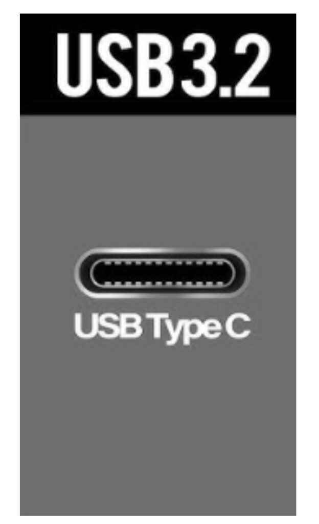
USB 3.2 Gen 2 (10 Gbps) doesn’t simply send raw binary data down a wire. Raw binary long strings of 1s or 0s causes a problem: if you send a thousand 1s in a row, the receiver’s clock-recovery circuit loses synchronisation with no transitions to lock onto. To solve this, USB 3.2 Gen 2 uses 128b/132b encoding: every 128 bits of actual data are encoded into a 132-bit symbol by inserting extra bits to guarantee enough signal transitions. This overhead is why the theoretical 10 Gbps line rate translates to a practical throughput of about 900+ MB/s actual sustained read speed, as Ugreen themselves specify.
The physical wire carrying this signal is a differential pair: two wires, TX+ and TX−, carrying opposite-polarity versions of the same signal. Any electrical noise (like a power supply ripple or electromagnetic interference from nearby components) will affect both wires equally and since the receiver only looks at the difference between the two, the noise cancels out. This is called Common-Mode Rejection, and it’s why USB 3.2 can run at 10 Gbps over a cable rather than demanding laboratory-grade shielding.
Inside the docking station’s PCB, the hub controller chip a VIA Labs VL817 class device manages all of this. It has three core jobs: arbitration (deciding which downstream device gets bus time when multiple devices request it simultaneously), protocol conversion (translating between the host USB 3.2 Gen 2 channel and the individual downstream port speeds, some at 10 Gbps and some at 5 Gbps), and power management (enforcing the 900mA per-port current limit and activating overcurrent protection if a device draws too much).
ESD and Overcurrent Protection: The Safety Physics
Every port on the Ugreen hub has ±15 kV ESD (Electrostatic Discharge) protection. When you plug in a device that’s been charged with static electricity which happens constantly in dry environments a discharge pulse carries thousands of volts for a few nanoseconds. Without protection, this spike would destroy the hub controller’s input transistors. The protection circuit uses a TVS (Transient Voltage Suppressor) diode: under normal conditions it is reverse-biased and invisible to the circuit, conducting essentially no current. The moment a spike arrives, the diode clamps the voltage to a safe level by avalanche conduction, absorbing the pulse energy as heat and protecting the downstream IC. This same principle a device that normally blocks current but permits it under extreme conditions is found in nearly every consumer electronic port on the planet.
The hub also specifies surge protection and overcurrent protection as named features. The overcurrent protection circuit uses a current-sensing resistor in series with each downstream power rail; when current exceeds the threshold, a comparator circuit signals the hub controller’s GPIO (General Purpose Input/Output) pin, which then cuts power to that port by shutting off the power switch FET (Field-Effect Transistor). Again, the transistor here plays a second classical role in electronics: not logic switching, but power switching acting as an electronically controlled relay.
The Enclosure: Why Aluminum, Not Plastic?
The Ugreen hub is made from aluminum alloy + PVC, a combination that isn’t aesthetic it’s thermal and electromagnetic physics.
Aluminum has a thermal conductivity of approximately 205 W/m·K, compared to roughly 0.2 W/m·K for typical ABS plastic a factor of about 1,000×. The hub controller chip and the USB power switching FETs dissipate heat during operation. If they were enclosed in plastic, that heat would build up inside the shell, raising the junction temperature of the chips and accelerating their wear through a mechanism called electromigration where high-temperature electrons physically push metal atoms in chip interconnects out of place over time, eventually breaking the circuit. The aluminum shell conducts that heat away to its outer surface, where it dissipates into the air by convection, keeping the internals cool passively without any fan.
The second reason for aluminum is EMI (Electromagnetic Interference) shielding. USB 3.2 signals at 10 Gbps generate RF emissions in the GHz range. A conductive metal enclosure acts as a Faraday cage: external electromagnetic fields induce surface currents in the aluminum that exactly cancel the incoming field inside the cage (by Lenz’s Law), and internal emissions are similarly contained. This is why regulatory bodies require consumer electronics to pass EMI tests, and why you’ll find metal or metalised plastic enclosures on any high-speed data device. The PVC portions used on the cable sheathing and port surrounds provide electrical isolation between the aluminum body and the connector pins, preventing a ground loop that would otherwise create noise on the signal lines.
The Mac Mini M4 + Ugreen 11-in-1 Hub are a window into how modern physics quantum electrostatics in FinFETs, electromagnetic wave optics in EUV, thermodynamics in aluminum shells, and signal theory in differential pairs all converge inside two objects that together cost less than $700 and sit quietly on your desk doing extraordinary things.
read more – https://circuitprofessor.com/category/circuitprofessor-explanations/