
“How 60 years of semiconductor physics collapsed the distance between a Moon landing and your coffee table. “
- What Are These Two Machines? (Jump)
- The Raw Numbers, Side by Side (Jump)
- Rabbit Hole 1 — The Transistor as a Switch: From Hand-Built RTL to 40 nm CMOS (Jump)
- Why the Transistor?
- The AGC’s RTL Gates: Physics You Can Hold in Your Hand
- The ESP32-P4’s CMOS at 40 nm: Physics at the Edge of the Visible
- Rabbit Hole 2 — Memory: From Magnetically Woven Wire to Silicon Cells (Jump)
- Why Memory Defines the Machine
- AGC Core Memory: Physics Woven by Hand
- ESP32-P4 Memory: A Hierarchy Built for Speed
- The Crosspoint vs. The Pipeline: How Instructions Are Executed (Jump)
- AGC: A Hardwired Crosspoint Generator
- ESP32-P4: A Pipelined RISC-V Core with Extensions
- What the AGC Could Do That Still Deserves Respect (Jump)
- The Real Physics Lesson: Moore’s Law Is a Law About Atoms (Jump)
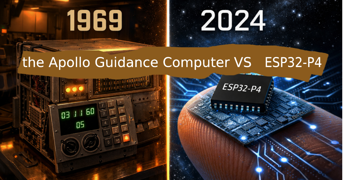
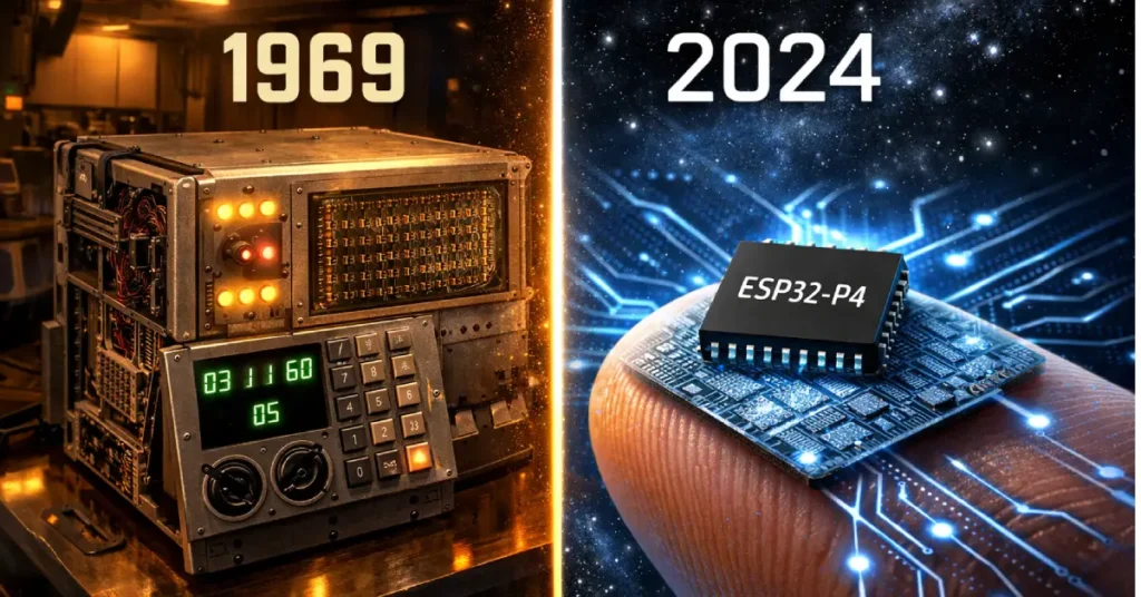
There is a chip you can buy right now for a few dollars roughly the size of a postage stamp that carries more raw computing power than the machine that guided three humans to the Moon and back in 1969. That chip is the Espressif ESP32-P4.
The machine it outperforms is the Apollo Guidance Computer (AGC), one of humanity’s most celebrated engineering achievements. This article does not just state that comparison as a fun fact and move on. It drills into why through the lens of physics, semiconductor engineering, and circuit architecture so you understand exactly what changed between 1969 and today.
What Are These Two Machines?
The Apollo Guidance Computer was a digital computer developed at the MIT Instrumentation Laboratory, designed solely to guide the Apollo spacecraft during navigation, orbital insertion, and lunar landing. It was first flown in 1966 and ran the Apollo 11 mission in July 1969. The entire computer measured about 2 cubic feet in volume, weighed approximately 70 pounds, and consumed around 70 watts of power.
The ESP32-P4 is a System-on-Chip (SoC) released by Espressif Systems in 2024–2025, currently in mass production. It is manufactured using TSMC’s 40 nm process technology and is intended for smart home, industrial automation, healthcare, and edge AI applications. The chip measures just a few millimeters across, costs a handful of dollars, and consumes a fraction of a watt.
The Raw Numbers, Side by Side
Before going deep, here is what the physics of each machine actually looks like on paper:
(ESP32-P4 vs the Apollo)
These numbers beg a deeper question: what physical and engineering realities produced this gap? There are two fascinating rabbit holes worth exploring how transistors shrank from hand-soldered components to atomic-scale switches, and how memory went from magnetically threaded wire loops to semiconductor cells. Both tell a story about physics that is far more interesting than the spec sheet.
Rabbit Hole 1 – The Transistor as a Switch: From Hand-Built RTL to 40 nm CMOS
Why the Transistor?
Everything in both computers (ESP32-P4 vs the Apollo) every calculation, every memory access, every clock tick reduces to transistors switching between two states: on (conducting current) and off (blocking current). This is not a metaphor.
A transistor is a three-terminal semiconductor device Base (or Gate), Collector (or Drain), and Emitter (or Source) where a small voltage or current at the control terminal determines whether a large current flows between the other two.
In the AGC, transistors served two concrete roles in every NOR gate circuit: they acted as fast electronic switches to pass or block logic signals, and in amplifier stages like sense amplifiers for core memory, they amplified tiny induced voltages into full logic-level signals.
The AGC’s RTL Gates: Physics You Can Hold in Your Hand
The AGC’s logic was built entirely from Resistor-Transistor Logic (RTL) NOR gate ICs, sourced from Fairchild Semiconductor. Each IC packaged in a metal flat-pack roughly the size of a fingernail contained just six transistors and eight resistors, implementing two 3-input NOR gates .
In an RTL NOR gate, if any one of the three inputs is driven high (logic 1), one of the three NPN bipolar transistors turns ON, pulling the output node to ground (logic 0). Only when all three inputs are low do all three transistors remain OFF, allowing the output to be pulled high through a resistor.
This is NOR logic at its most physical: the transistor is a literal switch that either short-circuits the output to ground or leaves it floating high.
The AGC used approximately 5,600 NOR gate ICs in its Block II version, with each board module holding two boards of 60 chips 240 NOR gates per module. NOR was chosen as the universal gate because any other logic operation (AND, OR, NOT, XOR, flip-flop) can be constructed purely from NOR gates, which meant NASA needed only one type of IC in the entire computer a critical reliability decision.
The total transistor count across all AGC ICs was approximately 17,000 transistors, which puts it architecturally between the Z80 microprocessor (8,500 transistors) and the Intel 8086 (29,000 transistors).
Each IC cost between $20–$30 (approximately $150 in today’s value). The AGC’s production consumed 60% of the entire United States’ integrated circuit output in 1963 . That is not an exaggeration this one computer program bootstrapped an entire semiconductor industry.
(back to menu)
The ESP32-P4’s CMOS at 40 nm: Physics at the Edge of the Visible
The ESP32-P4 is built on TSMC’s 40 nm CMOS (Complementary Metal-Oxide-Semiconductor) process. Here the transistor has evolved from a bipolar NPN device (AGC) into a MOSFET (Metal-Oxide-Semiconductor Field-Effect Transistor).
In a MOSFET, the control terminal (Gate) is electrically insulated from the channel by an extremely thin layer of silicon dioxide at 40 nm, this oxide layer is only a few atoms thick. When a voltage is applied to the Gate, it creates an electric field that attracts or repels charge carriers in the channel below, switching the transistor on or off without any base current being consumed.
“40 nm” refers to the gate length the physical distance between the source and drain of the transistor. At 40 nm, roughly 2,500 of these transistors placed end-to-end would span the width of a single human hair. This packing density allows the ESP32-P4 to integrate hundreds of millions of transistors on a die area of just a few square millimeters.
The CMOS architecture pairs each NMOS transistor with a PMOS transistor: when one is ON the other is OFF, meaning the circuit only draws significant current during the actual switching moment this is why the ESP32-P4 consumes milliwatts instead of the AGC’s 70 watts.
The RISC-V dual-core HP processor in the ESP32-P4 runs at up to 400 MHz with a 32-bit data path, an FPU (Floating Point Unit), and a custom hardware loop instruction extension called Xhwlp that reduces loop overhead in signal processing algorithms. A second LP (Low-Power) RISC-V core runs at up to 40 MHz and stays active when the main cores sleep, managing I/O and sensor polling.
This power architecture big cores for heavy lifting, small core for idle-state monitoring has no equivalent in the AGC, which operated at a flat 70 W regardless of task load.
📖 Read more — RISC-V ISA Foundation: https://riscv.org/technical/specifications/
📖 Read more — Transistor physics (MOSFET): https://en.wikipedia.org/wiki/MOSFET
📖 Read more — RTL Logic history: https://en.wikipedia.org/wiki/Resistor%E2%80%93transistor_logic
Rabbit Hole 2 Memory: From Magnetically Woven Wire to Silicon Cells
Why Memory Defines the Machine
In both computers, memory is not a passive storage room it is the architectural heartbeat. In the AGC, the memory timing cycle determined everything: how fast instructions executed, how many calculations per second were possible, and even the physical structure of the CPU’s datapath . The AGC’s entire instruction execution timing 11.72 microseconds per memory cycle, 12 time-steps per cycle was dictated not by the transistors but by the physical properties of magnetized ferrite rings .
AGC Core Memory: Physics Woven by Hand
The AGC used two types of memory, both relying on magnetic core technology. The erasable core memory (RAM) stored 2,048 16-bit words, where each bit was held in a tiny doughnut-shaped ferrite ring (a “core”) roughly 1 mm in diameter.
A ferrite core can be magnetized in one of two directions (clockwise or counterclockwise), representing a logical 1 or 0. To read a bit, a current pulse is sent through a wire threaded through the core, trying to force it into the “0” state. If the core was already 0, nothing happens. If it was 1, it flips to 0 and induces a tiny voltage pulse in a sense wire that pulse is detected and amplified by transistor-based sense amplifier circuits. The critical physics problem: reading a memory bit destroys it, because the act of sensing forces the core into the 0 state. This is why the AGC had to re-write every word back to memory after each read, adding extra clock cycles to every instruction .
The AGC’s ROM (core rope memory) was a masterpiece of physical encoding. Programmers could not type code into a compiler instead, wires were physically threaded through or around magnetic cores by hand by teams of workers (often called “little old ladies” in MIT folklore).
A wire passing through a core represented a binary 1; a wire passing around it represented a binary 0. The entire 36,864-word Apollo 11 flight software navigation algorithms, abort routines, landing sequences was permanently encoded as a physical weave of approximately 145,000 lines of code woven into wire. Once woven, the ROM could not be changed. The wiring was then embedded in cast epoxy plastic for protection.
ESP32-P4 Memory: A Hierarchy Built for Speed
The ESP32-P4 uses a two-level cache memory hierarchy built entirely from semiconductor SRAM and connected via high-speed on-chip buses. At the top level, the CPU cores access 8 KB of Zero-Wait Tightly-Coupled Memory (TCM) this memory sits physically adjacent to the processor pipeline, with no cache latency, allowing the CPU to read a data word in a single clock cycle (2.5 nanoseconds at 400 MHz). This is 4,680 times faster than the AGC’s 11.72 microsecond memory cycle time.
Below TCM sits 768 KB of on-chip HP SRAM accessible via AHB and AXI buses (standard ARM-style on-chip interconnects), plus 16 KB of LP SRAM for the low-power core. For applications needing larger data buffers such as video frame storage or audio DSP the ESP32-P4 can stack 16 MB or 32 MB of PSRAM directly inside its package, accessed at high speed without leaving the chip package.
The ESP32-P4 also features two independent DMA controllers (GDMA-AHB and GDMA-AXI) that move data between peripherals and memory without burdening the CPU a concept entirely absent in the AGC, where every data transfer consumed CPU time.
📖 Read more — SRAM vs DRAM physics: https://en.wikipedia.org/wiki/Static_random-access_memory
📖 Read more — AGC Core Rope Memory: http://www.righto.com/2019/01/inside-apollo-guidance-computers-core.html
📖 Read more — AGC full NOR gate CPU walkthrough: http://www.righto.com/2019/09/a-computer-built-from-nor-gates-inside.html
The Crosspoint vs. The Pipeline: How Instructions Are Executed
AGC: A Hardwired Crosspoint Generator
When the AGC executes an instruction like ADS (Add to Storage), it does not have a modern pipeline. Instead, a hardwired crosspoint generator a matrix of NOR gate logic takes the current sub-instruction and time-step as inputs and generates specific control pulses that physically gate registers onto the 16-bit write bus . For each of 12 timing steps (T1–T12), specific signals like A2X (copy accumulator to X register), RG (read memory buffer G), and WY (write to Y adder input) are asserted in a precise sequence .
The adder the only arithmetic operation the AGC can do in hardware then computes the sum of X and Y registers and routes it back through the bus . There is no branch prediction, no out-of-order execution, no speculative fetch. The machine proceeds step by step, constrained entirely by the 11.72 µs magnetic core memory timing cycle.
ESP32-P4: A Pipelined RISC-V Core with Extensions
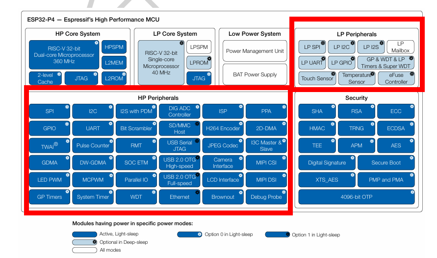
The ESP32-P4’s RISC-V HP cores execute instructions through a multi-stage pipeline, meaning multiple instructions are in different stages of fetch, decode, execute, and write-back simultaneously. The core implements the RV32IMAFCZc ISA Integer, Multiply, Atomic, Float, Compressed, and Bit-manipulation extensions plus the custom Xhwlp hardware loop instruction. Hardware loops eliminate the overhead of decrement-and-branch instructions in DSP inner loops, a technique critical for real-time signal processing. The chip also includes a Pixel Processing Accelerator (PPA) for 2D graphics, an H.264 video encoder, a JPEG codec, and a full Image Signal Processor (ISP) for camera input all as dedicated silicon blocks that run in parallel with the CPU.
What the AGC Could Do That Still Deserves Respect
None of this diminishes what the AGC achieved. It ran a real-time operating system with preemptive priority scheduling designed by J. Halcombe Laning that saved the Apollo 11 landing when a software overload triggered the infamous 1202 alarm during descent.
The operating system automatically shed lower-priority tasks and kept the critical guidance loop running entirely autonomously, 384,000 km from Earth. The AGC also connected to 227 interface circuits throughout the spacecraft, handling inertial measurement units, thrusters, radar, and the DSKY keyboard . The ESP32-P4 has 55 GPIO pins; the AGC had 227 real-time spacecraft interfaces.
The AGC’s software approximately 1,400 person-years of effort, led by Margaret Hamilton who received the Presidential Medal of Freedom for it was physically woven into rope memory by hand and could not be patched in flight. The ESP32-P4 supports over-the-air firmware updates via Wi-Fi. Both approaches represent the absolute cutting edge of their era’s constraints.
📖 Read more — Apollo Guidance Computer Wikipedia: https://en.wikipedia.org/wiki/Apollo_Guidance_Computer
📖 Read more — Margaret Hamilton and AGC software: https://en.wikipedia.org/wiki/Margaret_Hamilton_(software_engineer)
📖 Read more — ESP32-P4 Official Datasheet: https://documentation.espressif.com/esp32-p4-chip-revision-v1.3_datasheet_en.pdf
The Real Physics Lesson: Moore’s Law Is a Law About Atoms
The distance between these two machines is not primarily a story about better engineers. It is a story about how close to atomic scale humans have learned to carve silicon. In 1969, the AGC’s transistors were fabricated at the scale of hundreds of micrometers visible under a basic optical microscope.
In 2024, the ESP32-P4’s transistors at 40 nm are 2,500 times smaller in gate length, and the industry has since pushed to 3 nm in leading-edge chips. Each halving of transistor size roughly doubles the number you can fit in the same area (Moore’s Law), which is why the ESP32-P4 packs hundreds of millions of transistors where the AGC held 17,000.
The physical limit on this shrinkage is quantum mechanics: at gate lengths below ~5 nm, electrons tunnel through the insulating oxide layer regardless of whether the gate voltage commands them to stay put. The AGC’s transistors were large enough that quantum tunneling was irrelevant.
The ESP32-P4 at 40 nm is safely above the quantum tunneling cliff, but the industry is now engineering at nodes where that cliff is the central design constraint. Every chip you buy today exists in the gap between classical switching physics and quantum uncertainty a gap that has been narrowing for exactly 60 years, from the hand-wired NOR gates of Apollo to the invisible CMOS forests of the ESP32-P4.
📖 Read more — Moore’s Law: https://en.wikipedia.org/wiki/Moore%27s_law
📖 Read more — Quantum tunneling in transistors: https://en.wikipedia.org/wiki/Quantum_tunnelling
📖 Read more — TSMC 40nm process: https://en.wikipedia.org/wiki/40_nm_process
Read more – https://circuitprofessor.com/category/circuitprofessor-explanations/